Programmable Logic Device With On-Chip User Non-Volatile Memory

a programmable logic and user technology, applied in the field of integrated circuits, can solve the problems of much slower power-on speed than a single chip non-volatile fpga, and achieve the effect of convenient us

Active Publication Date: 2016-09-22
GOWIN SEMICON CORP LTD
View PDF5 Cites 14 Cited by
  • Summary
  • Abstract
  • Description
  • Claims
  • Application Information

AI Technical Summary

Benefits of technology

[0011]In order to overcome the deficiency of prior art, the present invention proposes a programmable ...

Problems solved by technology

However, it is much slower than a single c...

Method used


Image

  • Programmable Logic Device With On-Chip User Non-Volatile Memory
  • Programmable Logic Device With On-Chip User Non-Volatile Memory
  • Programmable Logic Device With On-Chip User Non-Volatile Memory

Examples


Embodiment Construction

[0029]The present invention is described in greater details below in conjunction with the figures, however, embodiments of the present invention are not limited by the description.

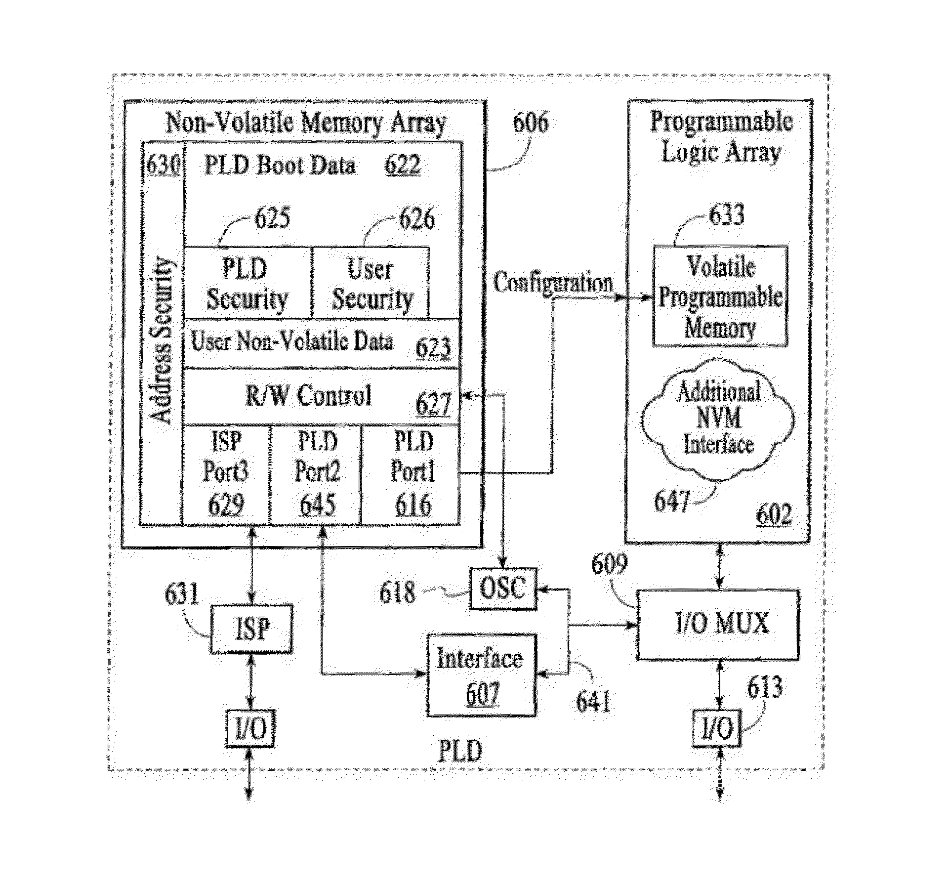
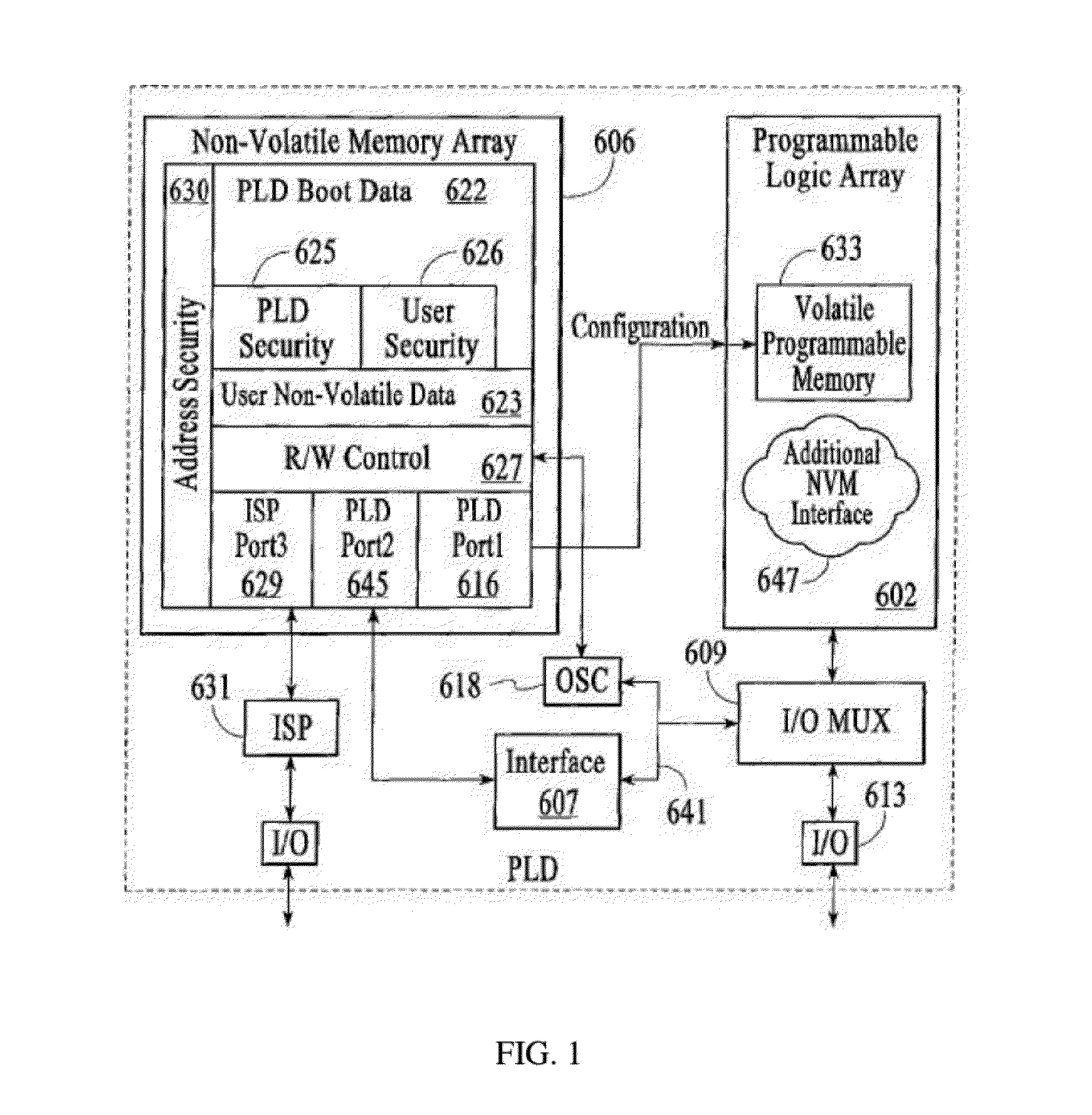
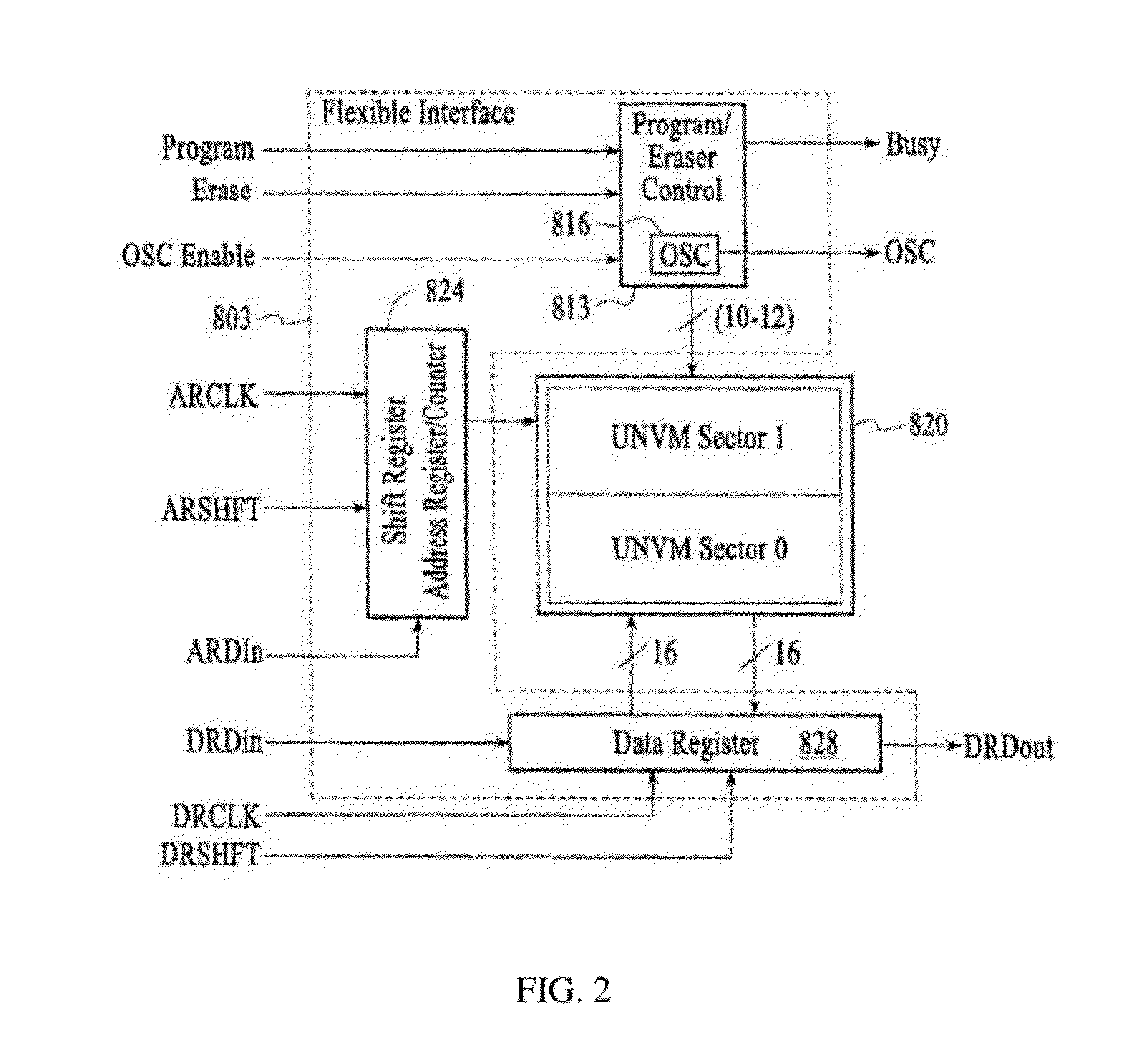
[0030]As shown in FIG. 3, a programmable logic device with on-chip user non-volatile memory, comprising:[0031]a programmable logic array, which is a user programmable logic array, comprising a SRAM array and a logic block with an interface; the SRAM array is used to store configuration data to control the logic block array in real time, therefore, the logic block can be formed to the function user desired;[0032]a non-volatile memory block, comprising one or more segments storing configuration data and one or more segments storing user data which is used during FPGA's normal operation after configuration; the non-volatile memory block has only one interface, and the non-volatile memory block connects to a programming controller through the interface;[0033]a programming controller, which can randomly access ...


PUM


Abstract

The present invention discloses a programmable logic device with on-chip user non-volatile memory, comprising: a programmable logic array, which is a user programmable logic array and comprises a SRAM array and a logic block array with an interface; the SRAM array is used to store configuration data to control the logic block array in real time, therefore, the logic block can be formed to perform the function a user desires; a non-volatile memory block, comprising one or more segments storing configuration data and one or more segments storing user data which is used during FPGA's normal operation after configuration; the non-volatile memory block has only one interface, and the non-volatile memory block connects to a programming controller through the interface; a programming controller, which can randomly access the non-volatile memory through a data bus, an address bus, and corresponding control signals.

Description

CROSS-REFERENCE TO RELATED APPLICATIONS[0001]The present application claims priority from Chinese Patent Application No. 201510117909.X filed Mar. 17, 2015, the disclosure of which is hereby incorporated herein by reference.TECHNICAL FIELD[0002]The present invention relates to the field of integrated circuits, more particularly to a non-volatile programmable logic device with on-chip user non-volatile memory.BACKGROUND[0003]After half of a century of development of integrated circuits, programmable logic devices applied in the field of integrated circuits have become ubiquitous, and computers, cellphones and other digital appliances become an indispensable part of the modern society structure. This is because modern computing, communication, manufacturing and transportation systems, including the Internet, all rely on the existence of integrated circuits. Over the years, integrated circuits constantly develop towards smaller external dimensions, so that each chip may encapsulate mor...

Claims


Application Information

Patent Timeline
IPC IPC(8): G06F3/06G06F13/16G06F13/40G06F13/10
CPCG06F3/0632G06F3/061G06F13/4068G06F13/102G06F13/1668G06F3/0685G06F9/4401G06F9/44505G06F15/7871
Inventor ZHU, JINGHUIKOW, SAN-TA
Owner GOWIN SEMICON CORP LTD
Why Eureka
Try Eureka