Electronic device having interference shielding structure

a shielding structure and electromagnetic technology, applied in the direction of individual energised antenna arrays, semiconductor/solid-state device details, printed circuit non-printed electric components association, etc., can solve the problem that noise cannot be generated and limit the effect of shielding function

Active Publication Date: 2019-06-20
SAMSUNG ELECTRONICS CO LTD
View PDF4 Cites 20 Cited by
  • Summary
  • Abstract
  • Description
  • Claims
  • Application Information

AI Technical Summary

Benefits of technology

[0008]Aspects of the disclosure are to address at least the above-mentioned problems and / or disadvantages and to provide at least the advantages described below. Accordingly, an aspect of the disclosure is to provide an electronic device including electromagnetic waves shielding structure having improved shielding function for an antenna module and elements.

Problems solved by technology

In this case, there is a limitation that noise cannot but be generated due to a gap between the antenna and the shield can.

Method used


Image

  • Electronic device having interference shielding structure
  • Electronic device having interference shielding structure
  • Electronic device having interference shielding structure

Examples


Embodiment Construction

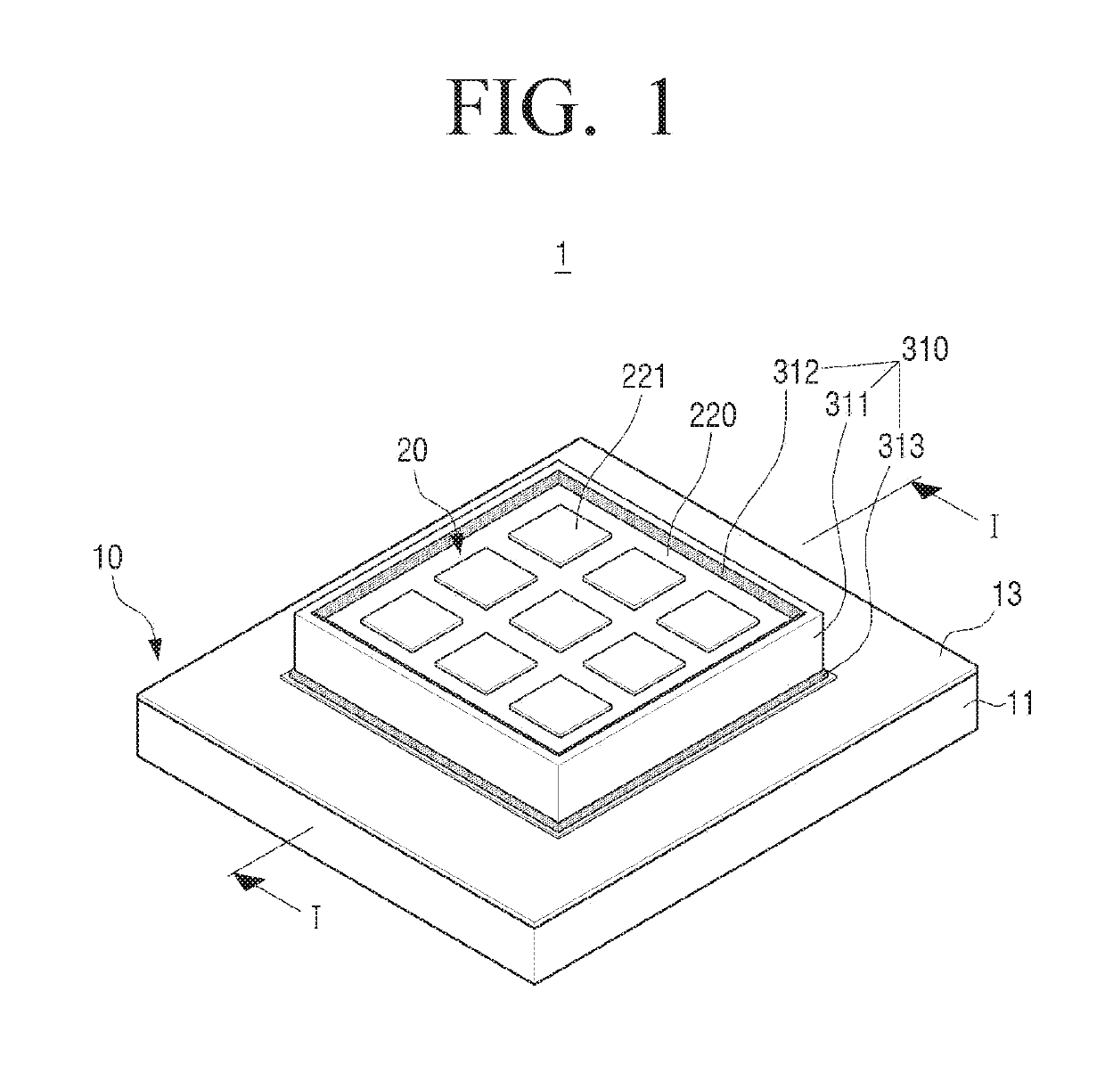
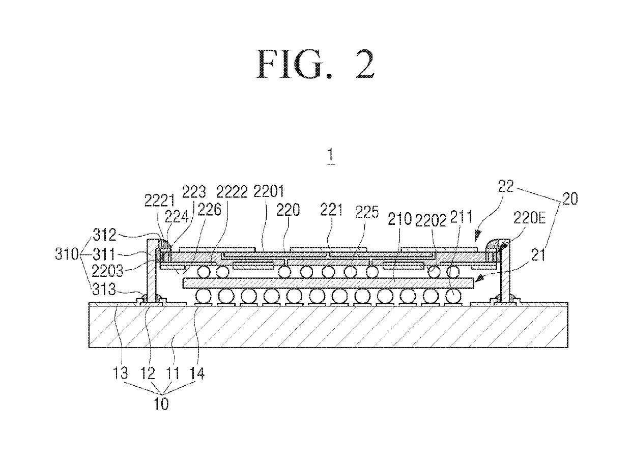
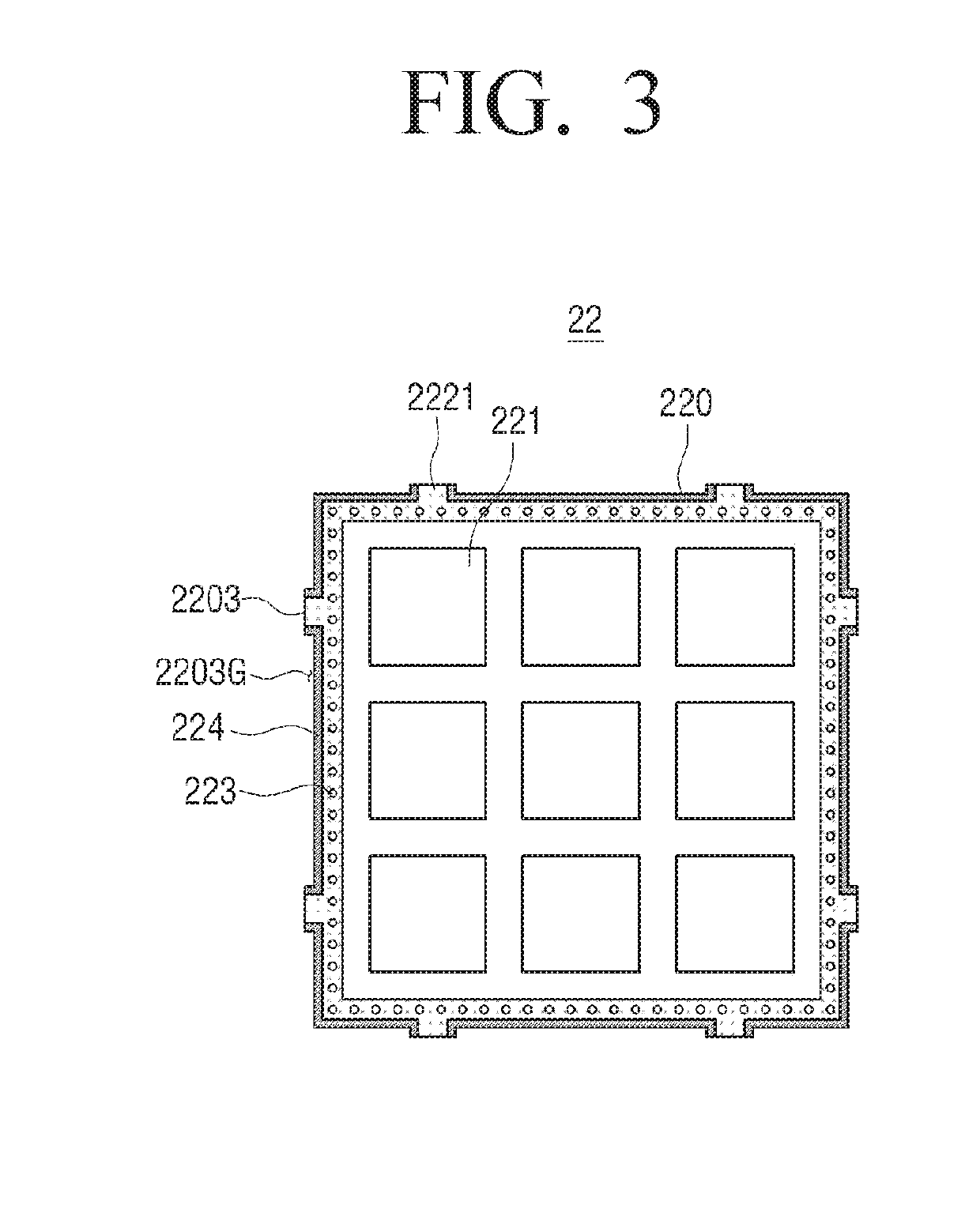
[0073]The following description with reference to the accompanying drawings is provided to assist in a comprehensive understanding of various embodiments of the disclosure as defined by the claims and their equivalents. It includes various specific details to assist in that understanding but these are to be regarded as merely exemplary. Accordingly, those of ordinary skill in the art will recognize that various changes and modifications of the various embodiments described herein can be made without departing from the scope and spirit of the disclosure. In addition, descriptions of well-known functions and constructions may be omitted for clarity and conciseness.

[0074]The terms and words used in the following description and claims are not limited to the bibliographical meanings, but, are merely used by the inventor to enable a clear and consistent understanding of the disclosure. Accordingly, it should be apparent to those skilled in the art that the following description of variou...


PUM


Abstract

An electronic device including an electromagnetic shielding structure is provided. The electronic device includes a printed circuit board, an antenna module, and an electromagnetic wave shielding structure. The antenna module includes a radio frequency integrated circuit mounted on the printed circuit board, and an array antenna coupled to an upper portion of the radio frequency integrated circuit. The electromagnetic wave shielding structure surrounds a side portion of the antenna module.

Description

CROSS-REFERENCE TO RELATED APPLICATION(S)[0001]This application is based on and claims priority under 35 U.S.C. § 119 of a Korean patent application number 10-2017-0173038, filed on Dec. 15, 2017, in the Korean Intellectual Property Office, the disclosure of which is incorporated by reference herein in its entirety.BACKGROUND1. Field[0002]The disclosure relates to an electronic device including electromagnetic interference shielding structure.2. Description of Related Art[0003]Recently, a demand for a portable electronic device such as a smartphone has been rapidly increasing in the electronic product market, and slimming and miniaturizing of electronic components mounted on portable devices have been in demand in a continuous manner. In order to realize the slimming and miniaturizing of the electronic components, a semiconductor packaging technique for integrating a plurality of individual circuit elements into one package, as well as a technique of reducing a size of an individual...

Claims


Application Information

Patent Timeline
Patent Type & Authority Applications(United States)
IPC IPC(8): H05K9/00H05K1/18H05K1/02H05K1/11H01Q21/06H01Q1/52H01Q1/22H01L23/66H01L23/552
CPCH05K9/0024H05K1/181H05K1/0218H05K1/111H01Q21/065H01Q1/526H01Q1/2283H01L23/66H01L23/552H05K2201/10098H05K2201/10378H05K2201/10734H05K3/341H05K2203/0126H01L2223/6677H01Q21/0093H01Q21/0087H05K2201/10371H05K2201/0715H01L2224/16227H01L2224/17181H01L2224/1703H01Q21/061H01Q3/08
Inventor HAN, EUNBONGKIM, HYEONHYANGBEAK, OHYUN
Owner SAMSUNG ELECTRONICS CO LTD
Why Eureka
Try Eureka