Electronic device having structure for eliminating parasitic emission

a technology of electronic devices and structures, which is applied in the construction details of electrical apparatus, substation equipment, and display/control unit casings, etc., can solve problems such as flickering and display malfunction, and achieve the effects of preventing display malfunction, removing parasitic emission, and improving antenna radiation performan

Active Publication Date: 2021-06-03
SAMSUNG ELECTRONICS CO LTD
View PDF0 Cites 2 Cited by
  • Summary
  • Abstract
  • Description
  • Claims
  • Application Information

AI Technical Summary

Benefits of technology

[0008]Aspects of the disclosure are to address at least the above-mentioned problems and / or disadvantages and to provide at least the advantages described below. Accordingly, an aspect of the disclosure is to provide an electronic device having a structure for eliminating parasitic emission.
[0009]Another aspect of the disclosure is to provide an electronic device having a structure for eliminating parasitic emission, capable of helping to improve the radiation performance of an antenna while preventing malfunction of a display.

Problems solved by technology

Due to absence of the ground, a malfunction such as flickering may be caused at the display.

Method used


Image

  • Electronic device having structure for eliminating parasitic emission
  • Electronic device having structure for eliminating parasitic emission
  • Electronic device having structure for eliminating parasitic emission

Examples


Embodiment Construction

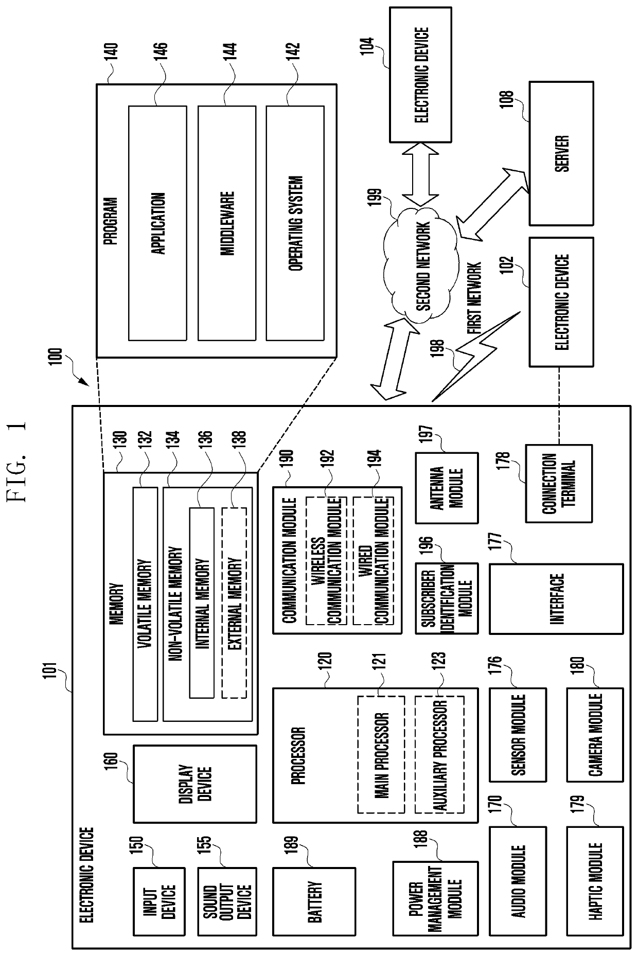
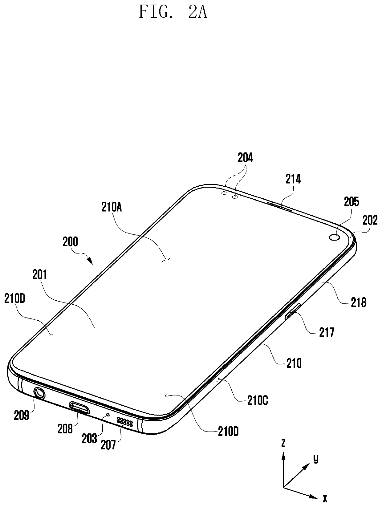
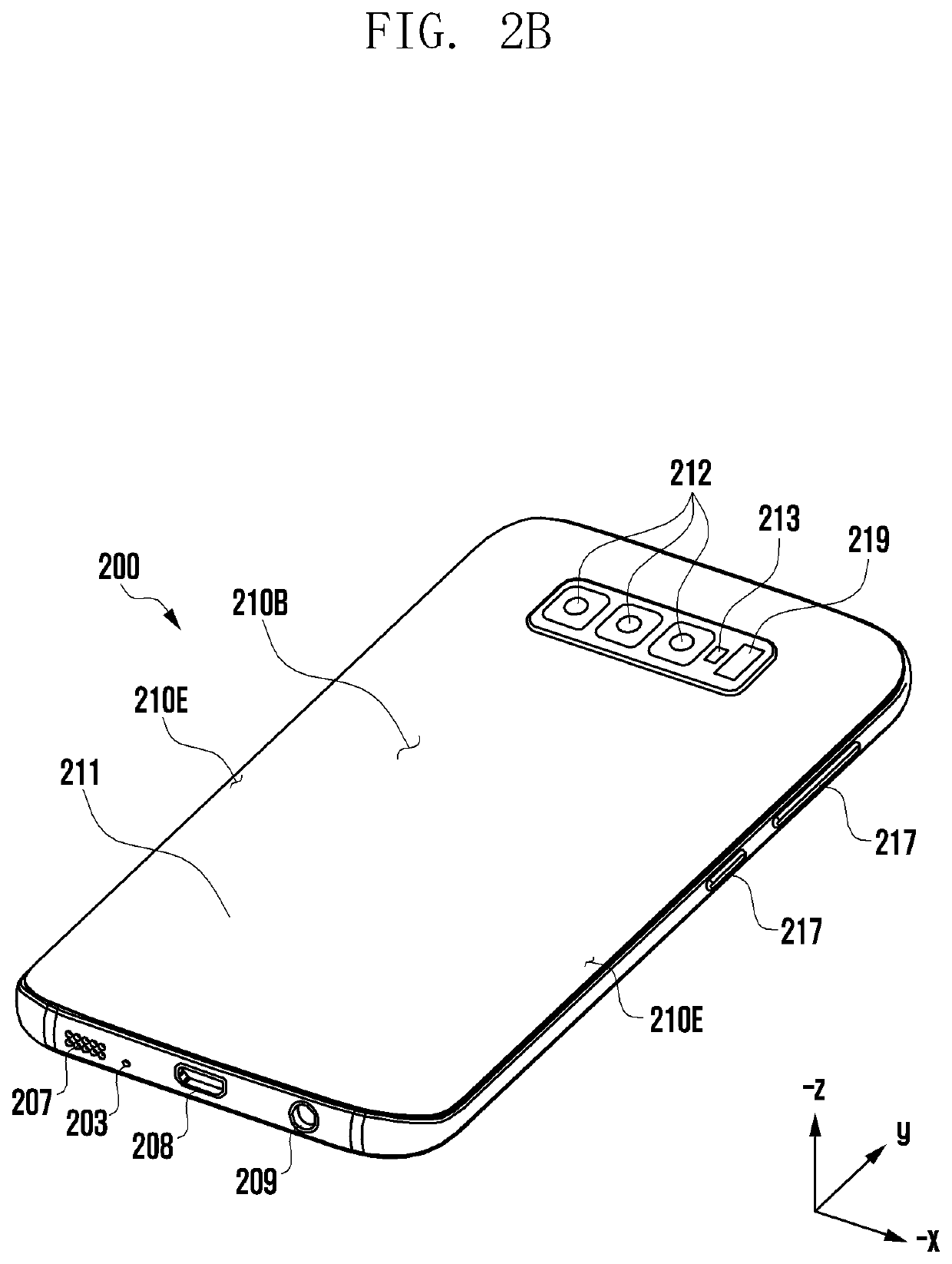
[0033]The following description with reference to the accompanying drawings is provided to assist in a comprehensive understanding of various embodiments of the disclosure as defined by the claims and their equivalents. It includes various specific details to assist in that understanding but these are to be regarded as merely exemplary. Accordingly, those of ordinary skill in the art will recognize that various changes and modifications of the various embodiments described herein can be made without departing from the scope and spirit of the disclosure. In addition, descriptions of well-known functions and constructions are omitted for clarity and conciseness.

[0034]The terms and words used in the following description and claims are not limited to the bibliographical meanings, but, are merely used by the inventor to enable a clear and consistent understanding of the disclosure. Accordingly, it should be apparent to those skilled in the art that the following description of various e...


PUM


Abstract

An electronic device for minimizing parasitic emission is provided. The electronic device includes a housing including a front cover, a rear cover located on the opposite side of the front cover, and a lateral member surrounding a space between the front cover and the rear cover, the lateral member having a first conductive portion formed on at least a portion thereof, a support member disposed in the space of the housing and including a second conductive portion having therein at least one opening, a display including a conductive sheet that is disposed between the front cover and the support member so as to be visible from an outside through at least a part of the front cover and is disposed to face the support member, and a wireless communication circuit electrically connected to the first conductive portion. The conductive sheet includes a first portion, a second portion disposed adjacent to the first portion, and a coupling that is partly connected between the first portion and the second portion. In case the front cover is viewed from above, the coupling is disposed at a position overlapping the opening.

Description

CROSS-REFERENCE TO RELATED APPLICATION(S)[0001]This application is based on and claims priority under 35 U.S.C. § 119 of a Korean patent application number 10-2019-0158528, filed on Dec. 2, 2019, in the Korean Intellectual Property Office, the disclosure of which is incorporated by reference herein in its entirety.BACKGROUND1 Field[0002]The disclosure relates to an electronic device having a structure for eliminating parasitic emission.2 Description of Related Art[0003]As functional gaps in recent electronic devices are remarkably reduced among manufacturers, the electronic devices are gradually being made slimmer to satisfy consumer interest, and are developed to have increased rigidity, to improve a design aspect thereof, and simultaneously to obtain a slim structure thereof.[0004]The electronic devices may include at least one antenna for supporting wireless communication services in various frequency bands. The at least one antenna may be disposed such that excellent radiation p...

Claims


Application Information

Patent Timeline
Patent Type & Authority Applications(United States)
IPC IPC(8): H01Q1/52H04M1/02H01Q1/24
CPCH01Q1/526H01Q1/243H04M1/0266H04M1/0277H04M1/026H05K9/0054H05K7/20963H05K5/0017H04B1/40
Inventor CHOE, JAEWONKIM, JIHOROH, MOOHYUNPARK, GYUBOKSEOL, KYUNGMOONAN, SEONGYONGJANG, KYIHYUN
Owner SAMSUNG ELECTRONICS CO LTD
Why Eureka
Try Eureka