Enhanced field emission from carbon nanotubes mixed with particles

a carbon nanotube and enhanced field technology, applied in the direction of electric discharge tube/lamp manufacturing, liquid/solution decomposition chemical coating, discharge tube luminescnet screen, etc., can solve the problems of poor growth uniformity, impede the utilization of low-temperature and generally inexpensive substrate materials, and none can practically deposit carbon nanotubes over large areas

Inactive Publication Date: 2004-09-28
SAMSUNG ELECTRONICS CO LTD
View PDF7 Cites 66 Cited by
  • Summary
  • Abstract
  • Description
  • Claims
  • Application Information

AI Technical Summary

Benefits of technology

The foregoing has outlined rather broadly the features and technical advantages of the present invention in order that the detailed description of the invention that follows may be better understood. Additional features and advantages of the invention will be described hereinafter which form the subject of the claims of the invention.

Problems solved by technology

All of the abovementioned techniques, however, have poor growth uniformity and none can practically deposit carbon nanotubes over large areas.
Furthermore, the growth conditions require relatively high temperatures, which impede their utilization with low-temperature and generally inexpensive substrate materials.
Another problem with using the abovementioned CNT growth techniques for generating the cathode material for field emission displays is that the density of the CNTs produced may be too high.
This method is very expensive, however, and requires growth on high-temperature substrates.

Method used


Image

  • Enhanced field emission from carbon nanotubes mixed with particles
  • Enhanced field emission from carbon nanotubes mixed with particles
  • Enhanced field emission from carbon nanotubes mixed with particles

Examples


example 1

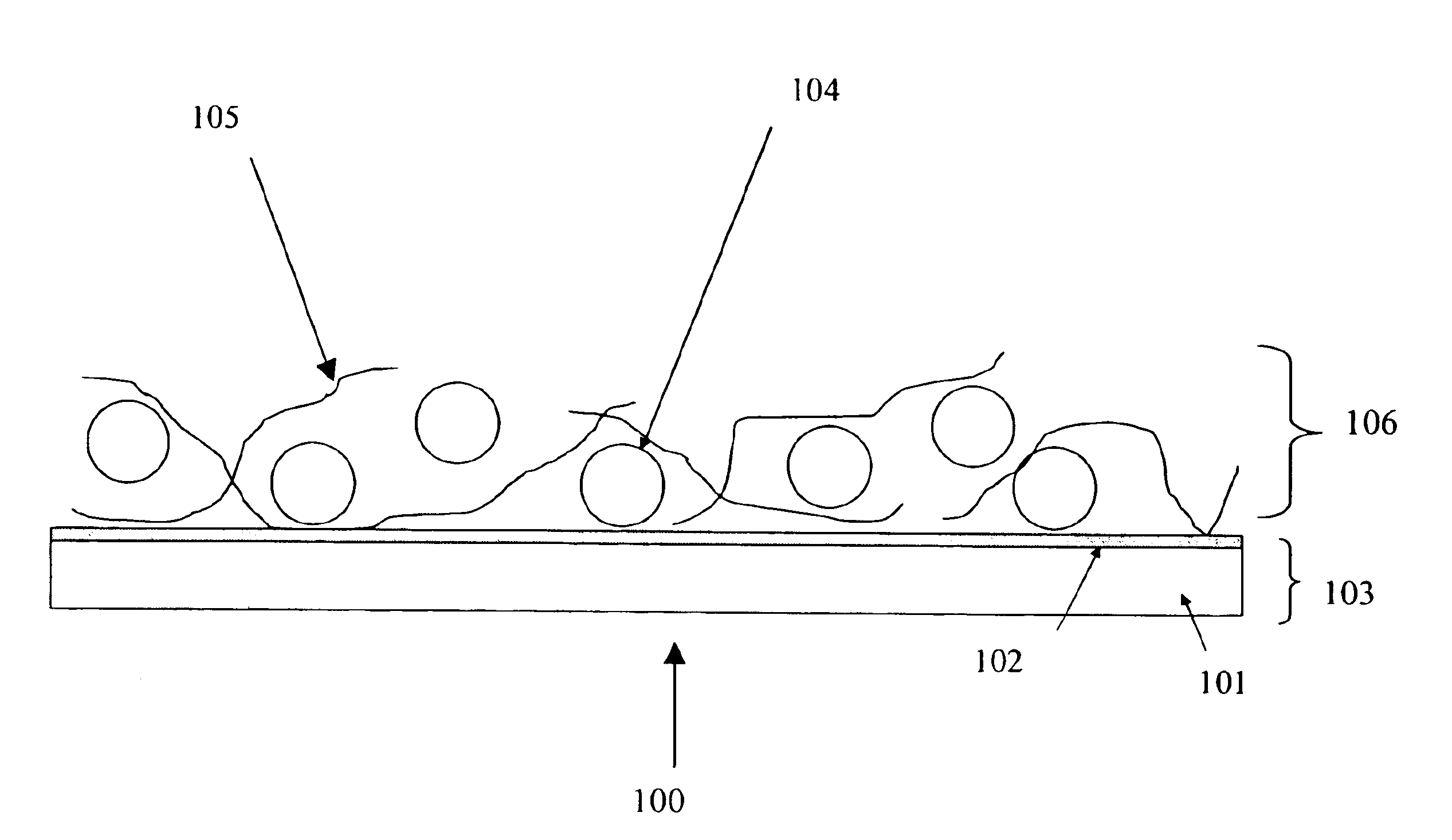
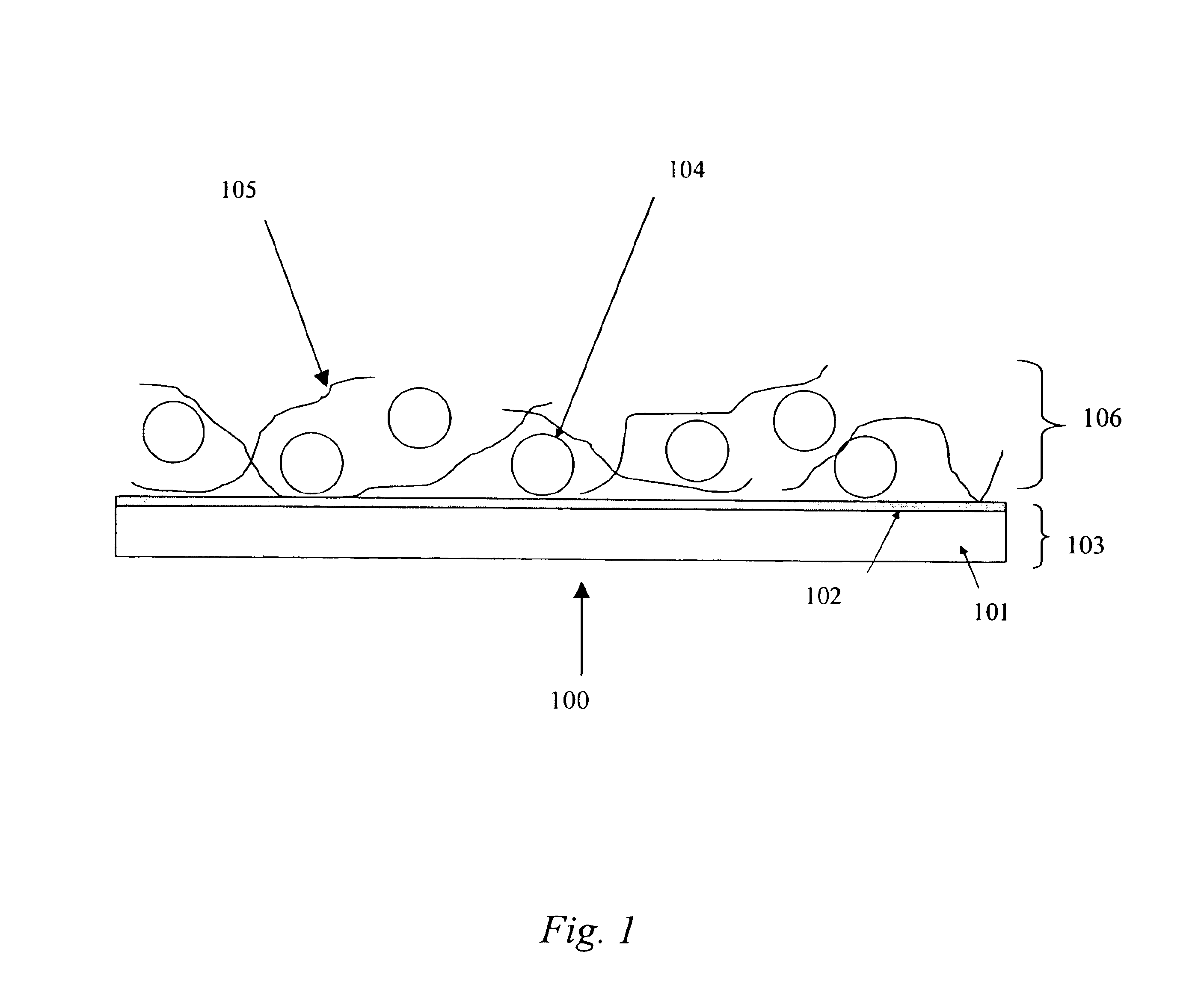
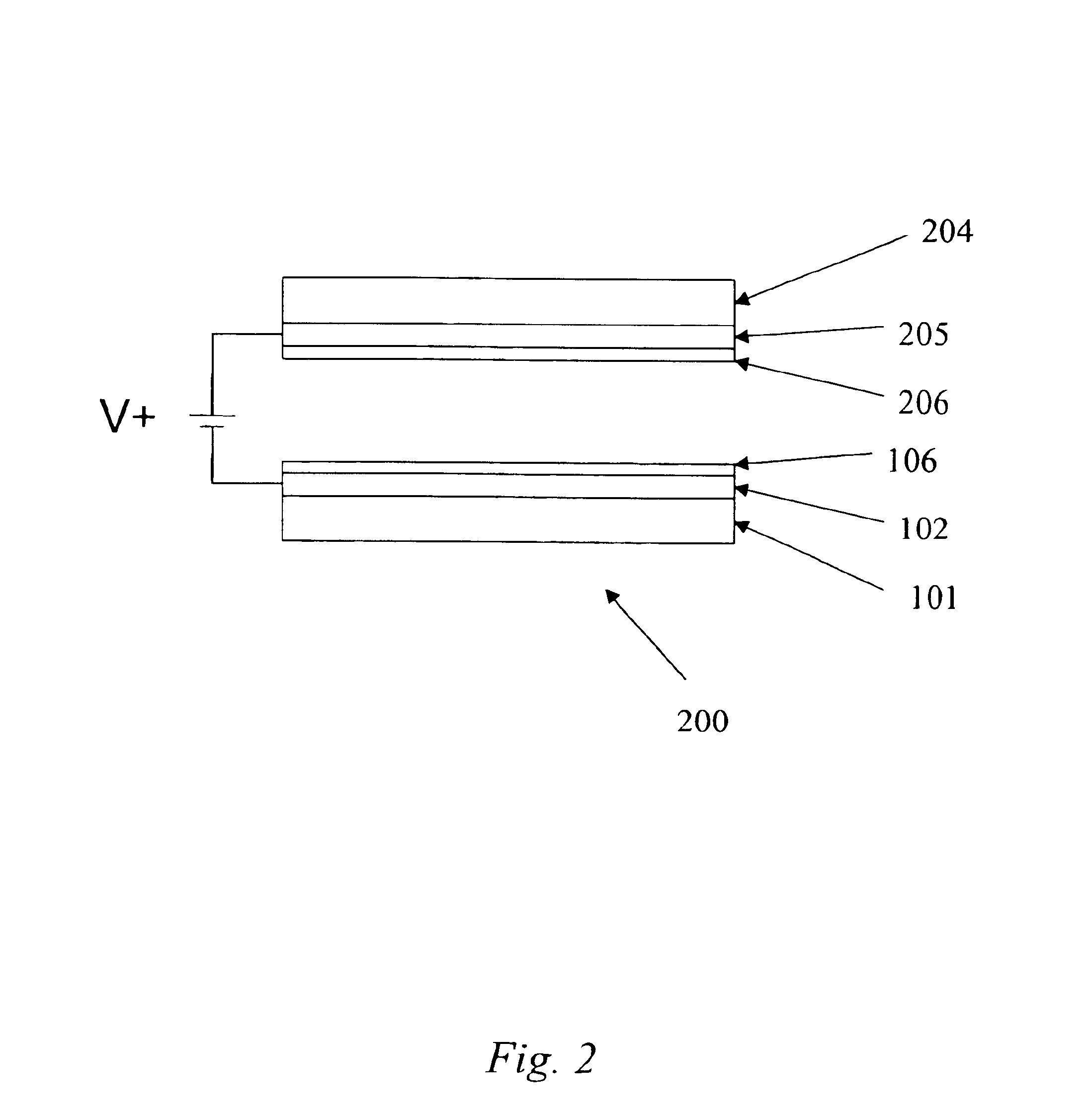
This example illustrates an embodiment of the present invention, wherein SWNTs are mixed with alumina (Al.sub.2 O.sub.3) nanoparticles to achieve an appropriate density, and then applied to a substrate and used as the cathode in a field emission display (see FIGS. 2 and 13). A detailed example of this embodiment is given in an effort to better illustrate the invention.

SWNTs were obtained from CarboLex, Inc., Lexington, Ky., USA. These SWNTs were about 1-2 nm in diameter and about 5-20 .mu.m in length. For the purposes of this example, it will be understood that SWNTs are simply a subset of CNTs and that in many cases the terms can be used interchangeably. Al.sub.2 O.sub.3 nanoparticles were obtained from Alfa Aesar, Ward Hill, Mass., USA. The nanoparticles are as small as 10-20 nm with a purity of 99.98%.

A simple ball mill was used to grind SWNT bundles. FIG. 3 is an illustrative diagram of this ball mill. The milling rate of this machine is on the order of about 50-60 revolutions p...

example 2

This example illustrates how activation processes are used to further enhance the field emission properties of the cathode of the present invention.

In an earlier disclosure (commonly assigned, co-pending U.S. patent application Ser. No. 10 / 269,577, filed Oct. 11, 2002, incorporated herein by reference), a process of "activating" the CNT film by applying an adhesive tape material to the film and then pealing the adhesive tape away was described. This also has the effect of lowering the density of the CNT fibers. This activation process was tried in combination with the CNT / alumina powder mixture described above. The results were consistent.

After a mixture of SWNTs and Al.sub.2 O.sub.3 is sprayed onto a substrate, an adhesive tape process was used to remove the top layer of the materials on the surface. In this method, clear tape was used to remove the mixture, although it is likely that there are many brands and varieties of adhesive tape that can be used with similar results. The ta...

example 3

This example illustrates some embodiments of the present invention which utilize clay particles.

As stated earlier, particles may be nanoparticles and they may also include porous materials such as porous silicon or one of several varieties of zeolite minerals. These particles may also include layered materials, such as clay particles. Examples of clays include, but are not limited to laponite, bentonite or hectorite. Clays are layered materials with spaces between the layers that can absorb water molecules or positive and negative ions (cations or anions) and undergo exchange interaction of these ions with solvents. Clays have very unique properties. When they are dried, the molecules or ions between the layers can come out, the gaps between the layers can close and the layer stack can shrink significantly. Correspondingly, when the clay particles are rehydrated, as shown in FIG. 13, the space between the clay particle layers 1301 expands.

Clay particles dispersed in solvents such as...


PUM

PropertyMeasurementUnit
thicknessaaaaaaaaaa
diametersaaaaaaaaaa
diametersaaaaaaaaaa

Abstract

The present invention is directed toward cathodes and cathode materials comprising carbon nanotubes (CNTs) and particles. The present invention is also directed toward field emission devices comprising a cathode of the present invention, as well as methods for making these cathodes. In some embodiments, the cathode of the present invention is used in a field emission display. The invention also comprises a method of depositing a layer of CNTs and particles onto a substrate to form a cathode of the present invention, as well as a method of controlling the density of CNTs used in this mixed layer in an effort to optimize the field emission properties of the resulting layer for field emission display applications.

Description

The present invention relates in general to field emission devices, and in particular to field emission devices comprising carbon nanotubes.BACKGROUND INFORMATIONCarbon nanotubes (CNTs) have intriguing physical and chemical properties which have consequently made them the object of numerous ongoing studies (Ajayan et al., Top. Appl. Phys., vol. 80, p. 391, 2001; Dai, Acc. Chem. Res., vol. 35, p. 1035, 2002). As a result of some of these studies, carbon nanotubes have been found to be excellent cathode materials for field emission displays because of their high aspect ratio and outstanding chemical inertness (U.S. Pat. No. 5,773,921). Single-wall carbon nanotubes (SWNTs) are hollow carbon fullerene tubes that have diameters from 5 angstroms to several nanometers (nm) and can be microns (.mu.m) long or longer. Multi-wall carbon nanotubes (MWNTs) are similar, but comprise more than one concentric layer of carbon forming the tube. It has been suggested that aligned carbon nanotubes may ...

Claims


Application Information

Patent Timeline
Patent Type & Authority Patents(United States)
IPC IPC(8): C23C18/12C23C18/16C23C18/00H01J9/02H01J19/06
CPCC23C18/1204C23C18/127H01J1/304H01J9/025B82Y10/00H01J2201/30469H01J2209/0223H01J2329/0455Y10S977/952Y10S977/939
Inventor MAO, DONGSHENGFINK, RICHARD LEEYANIV, ZVI
Owner SAMSUNG ELECTRONICS CO LTD
Why Eureka
Try Eureka