Stagger sensor and method for improving modulation transfer function

a modulation transfer function and sensor technology, applied in the direction of solid-state devices, instruments, material analysis, etc., can solve the problems of lowering the performance of the modulation transfer function (mtf), the size of the cells within the optical sensor cannot be changed, etc., and achieve the effect of improving the modulation transfer function

Active Publication Date: 2006-12-12
INTELLECTUAL VENTURES I LLC
View PDF3 Cites 0 Cited by
  • Summary
  • Abstract
  • Description
  • Claims
  • Application Information

AI Technical Summary

Benefits of technology

[0006]Accordingly, one object of the present invention is to provide a stagger sensor for improving modulation transfer function. The stagger sensor has a plurality of parallel-positioned sensing modules along the long axis that corresponds to each sensed primary color. The most important characteristic of the stagger sensor is that the first light-sensing cells of a first sensing module and the second light-sensing cells of a second sensing module each has a first end at an identical perpendicular position along the long axis. However, the first light-sensing cell and the second light-sensing cell each has a second end in different perpendicular positions along the long axis.
[0014]In brief, this invention utilizes the intrinsic structural advantages of a stagger sensor to increase the resolution along the X-axis. In addition, the modulation transfer function of each pixel is increased through the provision of reference digital data. Furthermore, the stagger sensor is able to increase the scanning resolution along the X-axis as well as the modulation transfer function of each pixel even without the provision of reference digital data.

Problems solved by technology

However, size of the cells within the optical sensor cannot be changed.
Therefore, using such a method to increase resolution may lower the performance of modulation transfer function (MTF).

Method used


Image

  • Stagger sensor and method for improving modulation transfer function
  • Stagger sensor and method for improving modulation transfer function
  • Stagger sensor and method for improving modulation transfer function

Examples


Embodiment Construction

[0025]Reference will now be made in detail to the present preferred embodiments of the invention, examples of which are illustrated in the accompanying drawings. Wherever possible, the same reference numbers are used in the drawings and the description to refer to the same or like parts.

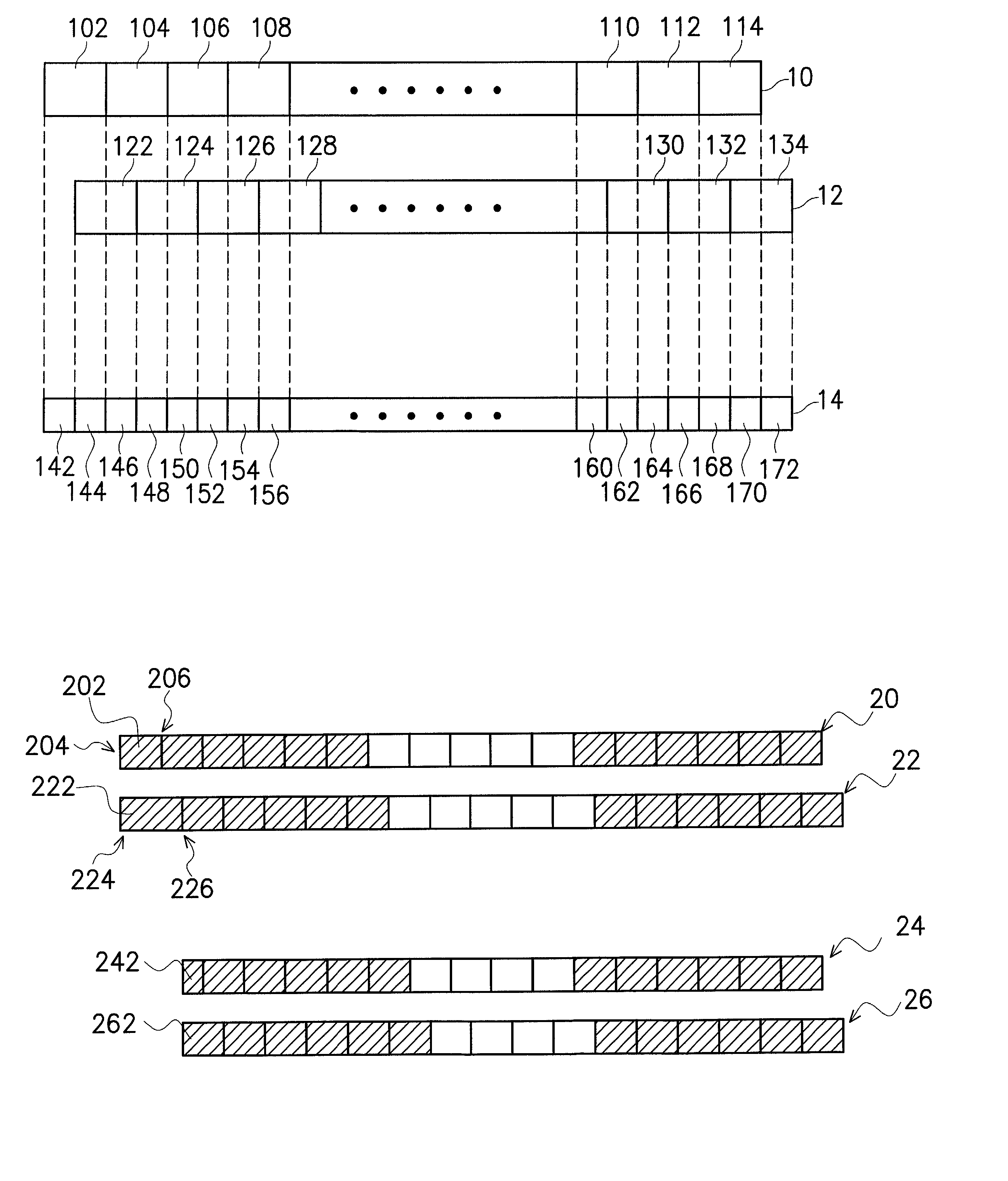
[0026]FIG. 1 is a diagram showing the relationship between pixel positions and the sensing cells within the stagger sensor according to one preferred embodiment of this invention. In this embodiment, the stagger sensor includes two groups of sensing modules 10 and 12 each having a multiple of light-sensing cells. The sensing module 10 includes light-sensing cells 102, 104, . . . , 114 while the sensing module 12 includes light-sensing cells 122, 124, . . . , 134. Due to a shift in position between the sensing module 10 and the sensing module 12 inside the stagger sensor, the portion of the scan object 14 captured by the light-sensing cells in the sensing module 10 does not overlap completely with the...


PUM


Abstract

A stagger sensor and a method for improving modulation transfer function. The method of using the stagger sensor for improving modulation transfer function can be applied to scan an object. The stagger sensor includes a plurality of sensing modules. The method of increasing scanning resolution includes retrieving reference digital data and processing digital data of a computed pixel obtained from an object scanning operation.

Description

BACKGROUND OF THE INVENTION[0001]1. Field of Invention[0002]The present invention relates to a stagger sensor and method for improving modulation transfer function. More particularly, the present invention relates to a stagger sensor and method for improving scanning resolution of a scanner.[0003]2. Description of Related Art[0004]Photocopiers, fax machines and scanners are common devices for capturing and converting images into electronic data for ease of printing, storage, transmission or image conversion. In general, optical sensors such as charge-coupled device (CCD) or contact image sensor (CIS) are used to extract image information. To capture a color image, the optical sensor normally consists of an array of CCD each capable of sensing at least the three primary colors red, green and blue. In a normal operation, all the CCD elements in the array are exposed to light for a predefined period. The amount of electric charge accumulated after the exposure is transferred to analogu...

Claims


Application Information

Patent Timeline
Patent Type & Authority Patents(United States)
IPC IPC(8): H04N1/04H01L27/00H04N1/193H04N1/40
CPCH04N1/193H04N1/1933H04N1/40H04N2201/0458
Inventor KUO, SHIH-ZHENG
Owner INTELLECTUAL VENTURES I LLC
Why Eureka
Try Eureka