

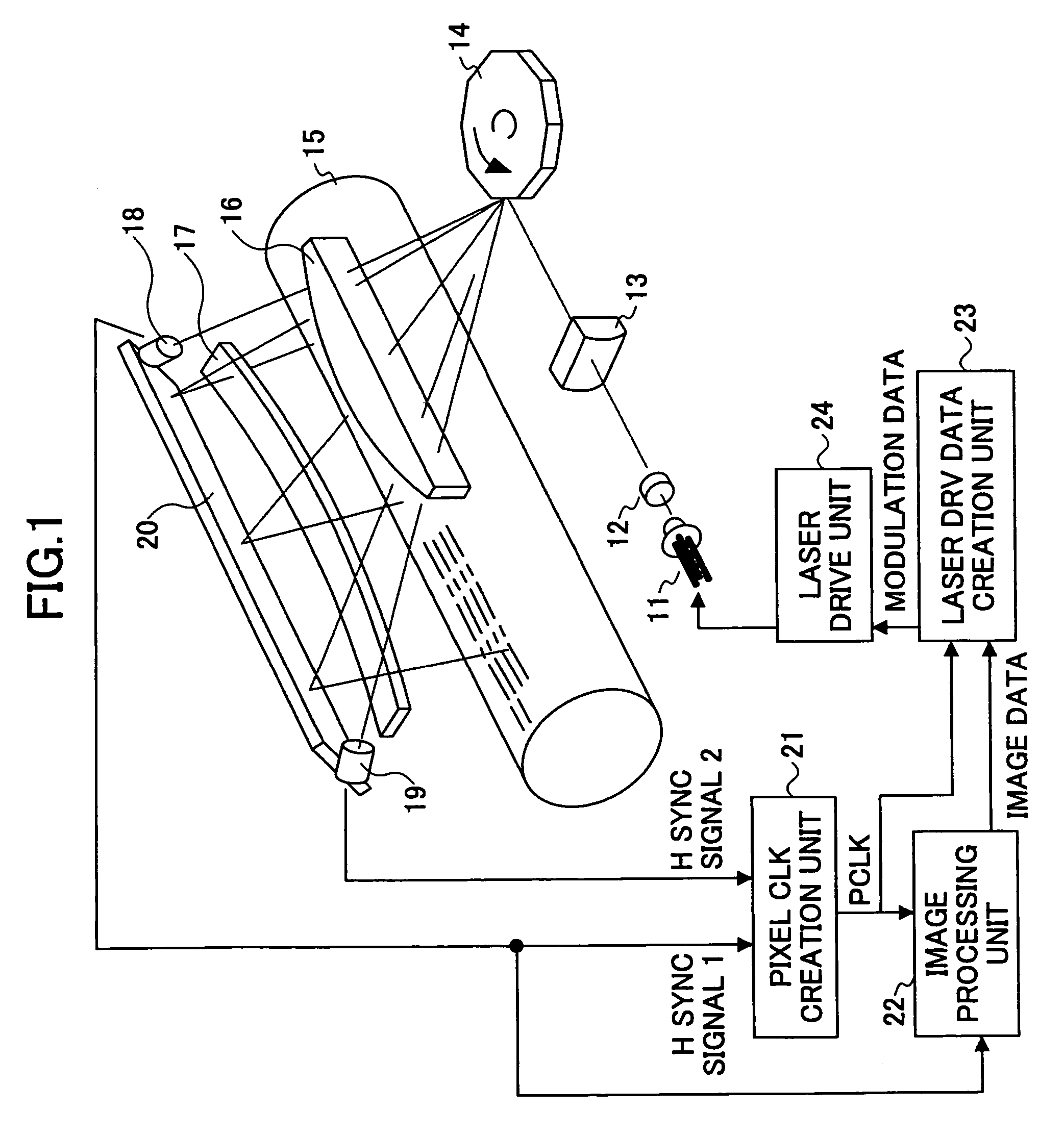
Pixel clock creation method, pixel clock creation device, optical scanning device, and image forming apparatus
a technology of pixel clock and creation method, which is applied in the direction of printing, visual presentation, instruments, etc., can solve the problems of deviation of exposure position, deformation of image quality, and irregular scanning speed of optical spots, so as to improve image quality, improve image quality, and improve the effect of image quality
- Summary
- Abstract
- Description
- Claims
- Application Information
AI Technical Summary
Benefits of technology
Problems solved by technology
Method used
Image

Examples
first embodiment
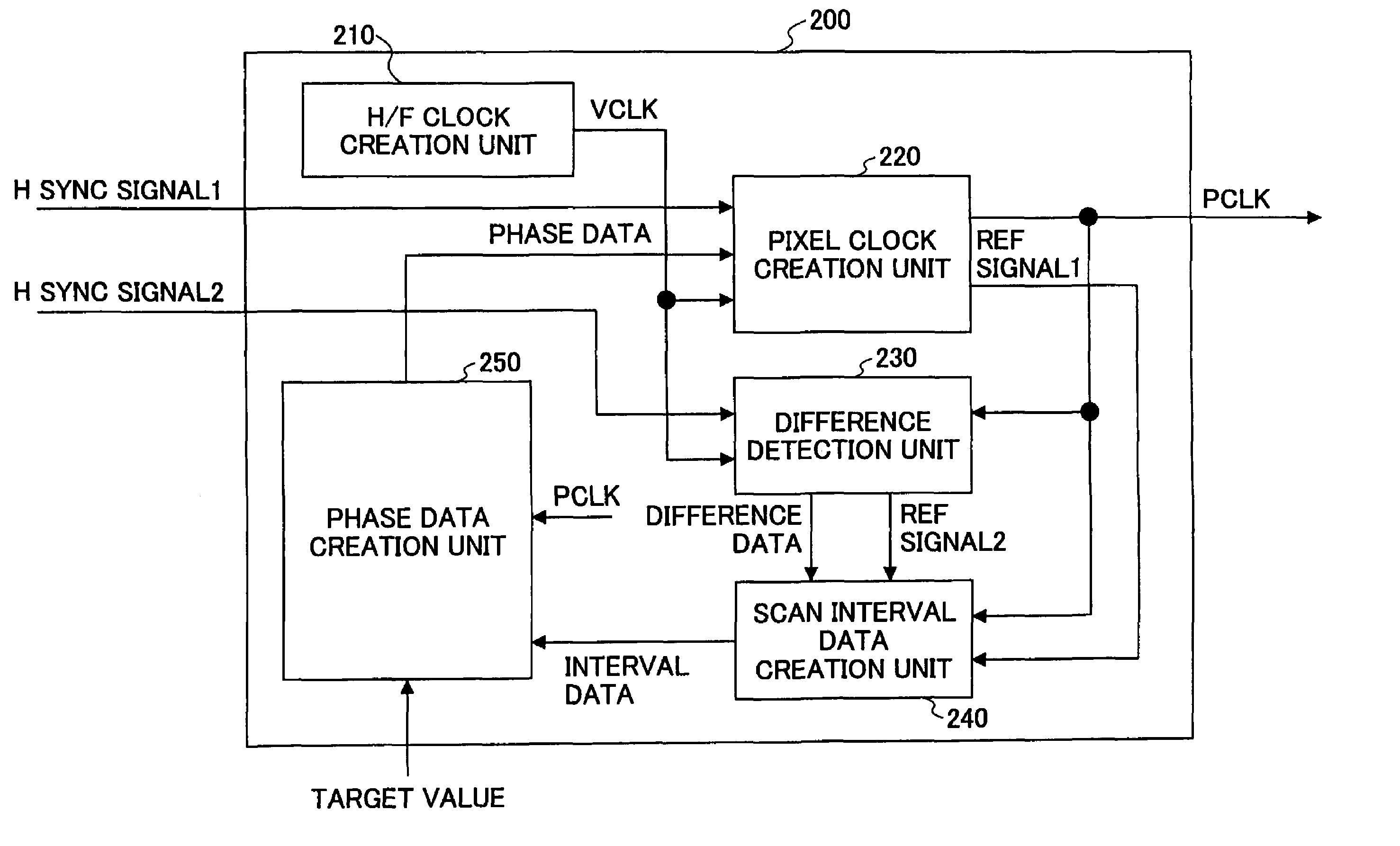
[0164]FIG. 14 is a block diagram of the detection unit 120 in FIG. 2.
[0165]The detection unit 120 comprises the detection data creation circuit 1213 which creates detection data from the output value and horizontal sync signal2 of counter (2) 1212 counted in falling of counter (1) 1211 and the high frequency clock VCLK counted in rising of the high frequency clock VCLK on the basis of the horizontal sync signal1, counter (1) 1211, and counter (2) 1212 in FIG. 14.
[0166]FIG. 15 and FIG. 16 show the case where it falls when the horizontal sync signal1 is in the state of “H” of VCLK.
[0167]Counter (2) 1212 are previously reset by 0 (b of FIG. 15, b of FIG. 16), next counter (1) 1211 are reset by 0 (c of FIG. 15, c of FIG. 16), and the count is carried out by what (a of FIG. 15, a of FIG. 16) the horizontal sync signal1 fell.
[0168]And when the horizontal sync signal2 is in the state of “H” of VCLK and it falls (d of FIG. 15), the count value of counter (1) 1211 and counter (2) 1212 can be...
second embodiment
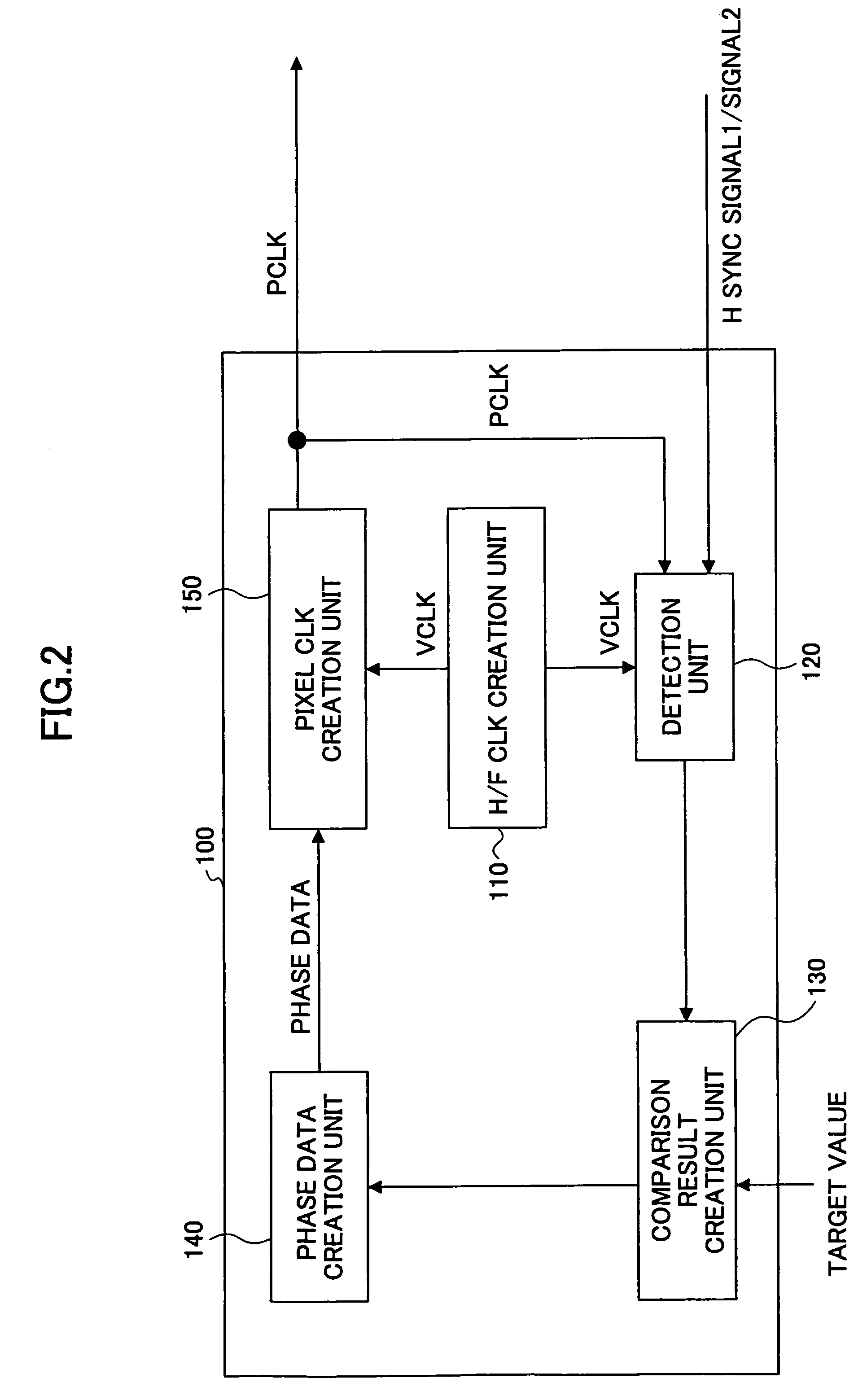
[0176]FIG. 19 is a block diagram of the detection unit 120 in FIG. 2.
[0177]The counter 1221 which counts the detection unit 120 in rising of the high frequency clock VCLK in FIG. 19. State creation circuit (1) 1222 which create the state signal 1 which shows the state of VCLK when the horizontal sync signal1 falls.
[0178]It comprises in the detection data creation circuit 1224 which creates detection data from state creation circuit (2) 1223 which create the state signal 2 of VCLK when the horizontal sync signal2 falls, the count value of the counter 1221, the state signal 1, and the state signal 2.
[0179]The example of composition of state signal creation circuit (1) 1222 is shown in FIG. 20.
[0180]State signal creation circuit (2) The composition of 1223 also becomes the same. The timing view of state signal creation circuit (1) 1222 of operation of FIG. 20 is shown in FIG. 21 and FIG. 22.
[0181]FIG. 21 shows the case where it falls when the horizontal sync signal1 is in the state of ...
third embodiment
[0202]FIG. 24 is a block diagram of the detection unit in FIG. 2.
[0203]In FIG. 24, the pixel clock PCLK is given from the pixel clock creation circuit 150 synchronizing with falling of the horizontal sync signal1.
[0204]Counter (1) 1231 is a counter which it is reset based on falling of the horizontal sync signal1, and is counted by PCLK. Counter (2) 1232 is a counter which it is reset based on rising of PCLK and counted in rising of the high frequency clock VCLK. Counter (3) 1233 is a counter which it is reset based on rising of PCLK and counted in falling of VCLK.
[0205]The detection data creation circuits 1234 are counter (1) 1231 when the horizontal sync signal2 falls, counter (2) 1232, and the circuit that creates detection data from the value of counter (3) 1233.
[0206]Counter (1) 1231 of FIG. 24, counter (2) 1232, and the timing of counter (3) 1233 of operation are shown in FIG. 25, FIG. 26, and FIG. 27. PCLK uses FIG. 25, FIG. 26, and FIG. 27 as 8 dividing clock of VCLK.
[0207]F...
PUM
 Abstract
Description
Claims
Application Information