

Epitaxial growth of CZT(S,Se) on silicon
a technology of czt(s, se) and silicon, which is applied in the manufacture of semiconductor/solid-state devices, electrical apparatus, and semiconductor devices, etc., can solve problems such as voltage problems in solar devices, and achieve the effects of enhancing the wettability of czt(s,se), and enhancing the wettability of epitaxial kesterite materials
- Summary
- Abstract
- Description
- Claims
- Application Information
AI Technical Summary
Benefits of technology
Problems solved by technology
Method used
Image

Examples
Embodiment Construction
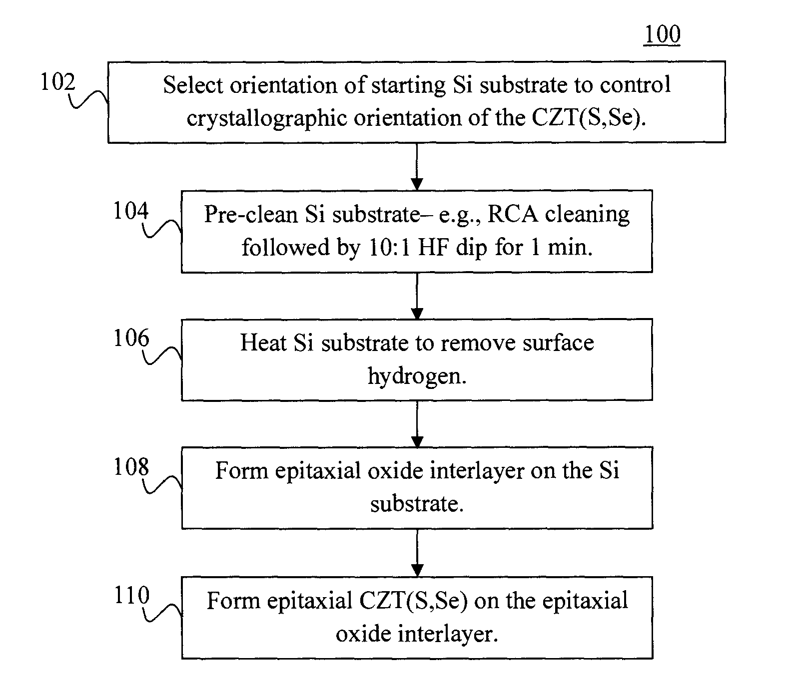
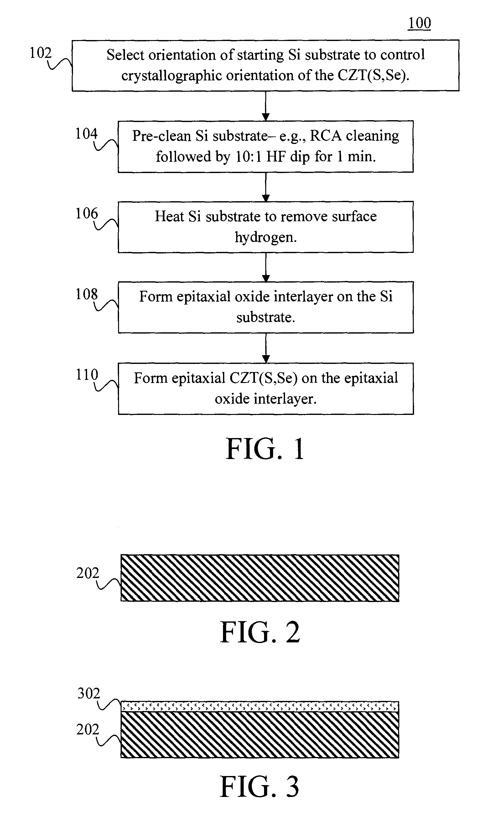
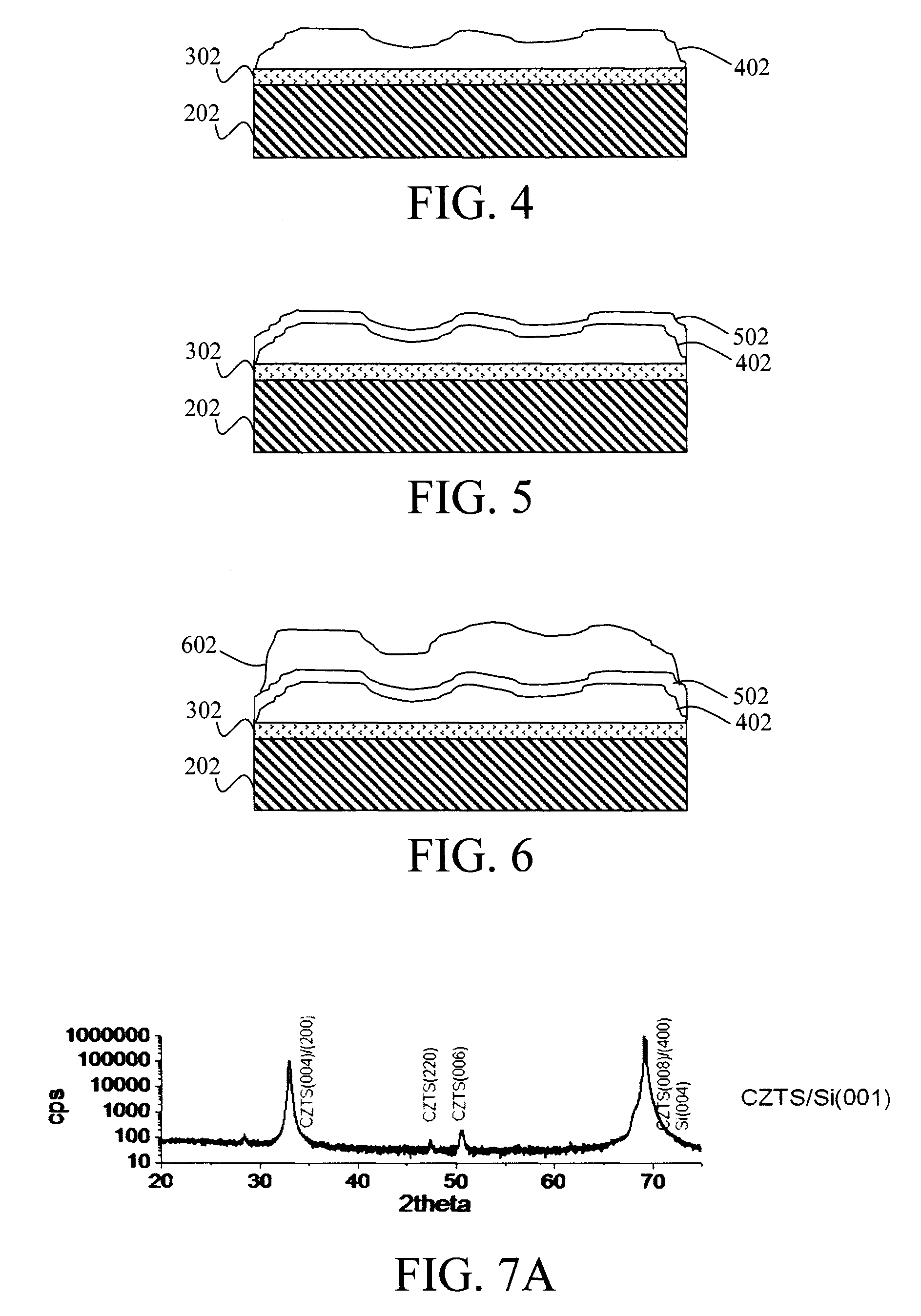
[0020]Provided herein are techniques for producing grain boundary-free epitaxial CZT(S,Se) materials on silicon (Si) substrates. As provided above, CZT(S,Se) materials are kesterites containing copper (Cu), zinc (Zn), tin (Sn), and at least one of sulfur (S) and selenium (Se). Epitaxy involves the growth of a crystalline material (in this case CZT(S,Se)) on a crystalline substrate (in this case a Si substrate). To be epitaxial, the atoms in the growing film must align themselves with those in the substrate so as to form a continuous atomic arrangement across the interface (i.e., the atomic planes in the film are a continuation of the atomic planes in the substrate).
[0021]Grain boundaries are the interfaces between grains in a polycrystalline material and have been correlated with recombination in other polycrystalline material systems. Grain boundaries in a CZT(S,Se) material are undesirable as they are thought to impede carrier mobility and / or introduce recombination centers, thus ...
PUM
| Property | Measurement | Unit |
|---|---|---|
| thickness | aaaaa | aaaaa |
| pressure | aaaaa | aaaaa |
| temperature | aaaaa | aaaaa |
Abstract
Description
Claims
Application Information