Supercharge Your Innovation With Domain-Expert AI Agents!

Sensing apparatus for detecting user touch

a technology for sensing apparatus and touch, which is applied in the field of sensing apparatus for detecting a user touch, can solve the problems of inability to recognize or misjudgment fingerprint patterns, low ease of use, and high hardware costs, so as to reduce the number of sensing elements nor the area of a sensing region, and prevent inconvenien

Inactive Publication Date: 2018-05-22
MSTAR SEMICON INC
View PDF7 Cites 1 Cited by
  • Summary
  • Abstract
  • Description
  • Claims
  • Application Information

AI Technical Summary

Benefits of technology

This approach reduces hardware costs and increases flexibility in packaging while maintaining sensing resolution, preventing inconveniences associated with small-area sensing regions and improving recognition accuracy.

Problems solved by technology

One drawback of such typical fingerprint recognition device is that, in order to coordinate with the size of the sensing region and to accomplish a sufficient sensing resolution, the number of sensing circuits involved is massive, hence resulting in a huge load on hardware costs.
Although such fingerprint recognition device is cheaper, it offers lower ease of use.
Further, the incapability of recognition or misjudgment of fingerprint patterns may occasionally occur if the user slides the fingertip at inappropriate speed.
In a typical fingerprint recognition device, each sensing element and the corresponding sensing circuit are connected by an independent connecting line, and so the number of connecting lines between the sensing region and backend circuits is inevitably enormous.
As such, if the sensing elements and the backend circuits are packaged in different hardware circuits, these two circuits are forced with huge numbers of external pins due to the enormous number of connecting lines in between, again leading to increased hardware costs.
However, such unavoidable packaging method limits the flexibility of hardware configuration and fabrication process selection to a certain extent.

Method used


Image

  • Sensing apparatus for detecting user touch
  • Sensing apparatus for detecting user touch
  • Sensing apparatus for detecting user touch

Examples


Embodiment Construction

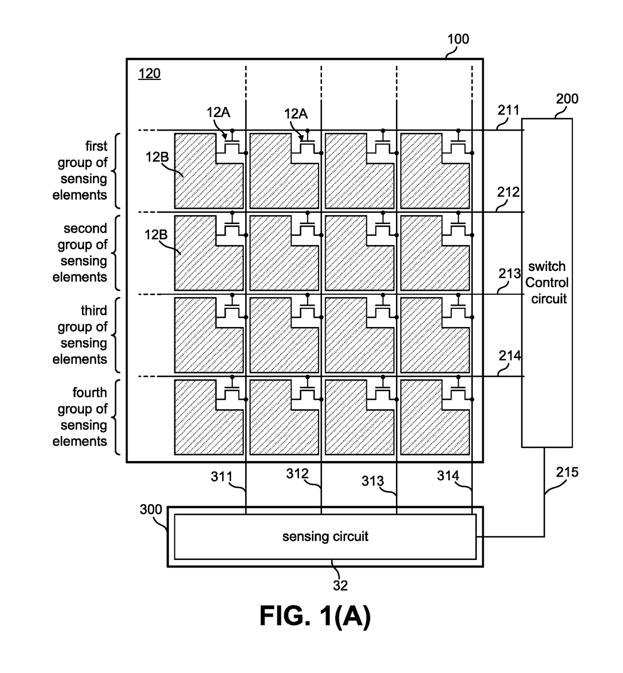
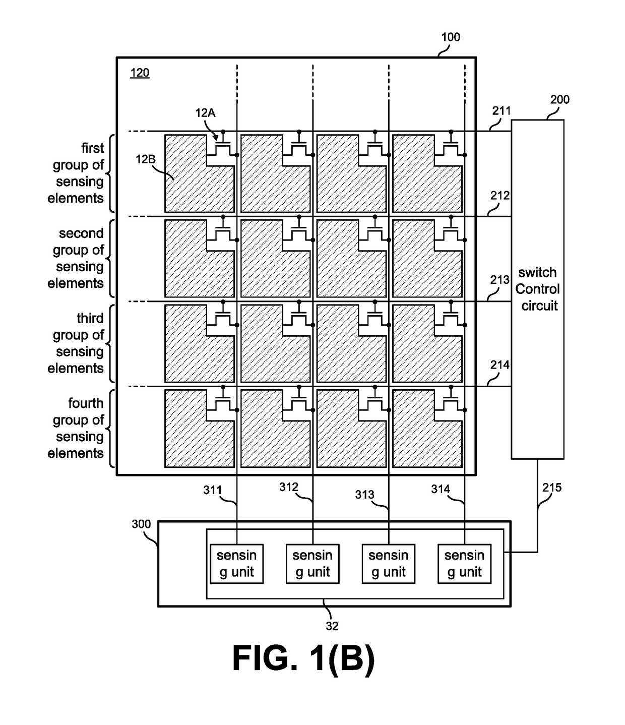
[0019]FIG. 1(A) shows a function block diagram of a sensing apparatus according to an embodiment of the present invention. The sensing apparatus includes a substrate 100, a switch control circuit 200, and an integrated circuit 300. In practice, the sensing apparatus may be an independent unit, or may be integrated into an electronic product that requires a touch sensing function for a user touch, such as a mobile phone, a laptop computer and a tablet computer. It should be noted that, for example but not limited to, the sensing apparatus of the present invention may be utilized for fingerprint recognition.

[0020]A thin-film transistor (TFT) structure 120 is formed on the substrate 100. The structure includes a plurality of TFT switches 12A and a plurality of sensing electrodes 12B (the shaded parts). In practice, the sensing electrodes 12B may be realized by a metal layer or a metal alloy layer in the TFT structure 120. Each of the sensing electrodes 12B correspond to one of the TFT ...


PUM


Abstract

A sensing apparatus includes a substrate, N groups of sensing elements formed on the substrate, a sensing circuit and a switch control circuit. Each group of the N groups of sensing elements includes a plurality of sensing elements. Each of the sensing elements includes a thin-film transistor (TFT) switch and a sensing electrode. The sensing electrode drives the N groups of sensing elements to sequentially generate N groups of sensing signals. By controlling the TFT switches, the switch control circuit controls a plurality of sensing electrodes included in one group of the N groups of sensing elements to be coupled to the sensing circuit.

Description

[0001]This application claims the benefit of Taiwan application Serial No. 104114240, filed May 5, 2015, the subject matter of which is incorporated herein by reference.BACKGROUND OF THE INVENTION[0002]Field of the Invention[0003]The invention relates to a sensing apparatus for detecting a user touch.[0004]Description of the Related Art[0005]To increase data security, many electronic products provide fingerprint recognition in the recent years. A most typical fingerprint recognition device includes a sensing region having an area of approximately 1 cm2 for a user to press a fingertip thereon. Below the sensing region are multiple sensing elements in a matrix arrangement. To adapt to gaps between two friction ridges, at least 100*100 (i.e., approximately 10000) sensing elements need to be provided in order to provide a sufficient sensing resolution. If self-capacitive sensing elements are adopted, sensing circuits in the same number as the sensing elements are usually provided in the...

Claims


Application Information

Patent Timeline
Patent Type & Authority Patents(United States)
IPC IPC(8): G06K9/00G06F3/041
CPCG06K9/0002G06V40/1306
Inventor HO, KAI-TING
Owner MSTAR SEMICON INC
Features
  • R&D
  • Intellectual Property
  • Life Sciences
  • Materials
  • Tech Scout
  • Unparalleled Data Quality
  • Higher Quality Content
  • 60% Fewer Hallucinations
Learn More