
Organic electroluminescent material, preparation method thereof and organic electroluminescent device
An electroluminescent material and electroluminescent technology, applied in the direction of luminescent materials, electro-solid devices, electrical components, etc., to achieve the effects of improving current characteristics, long device life, and high electron transmission efficiency
Patent Information
- Authority / Receiving Office
- CN · China
- Patent Type
- Applications(China)
- Current Assignee / Owner
- Publication Date
- 2018-07-13
- Estimated Expiration
- Not applicable · inactive patent
Smart Images
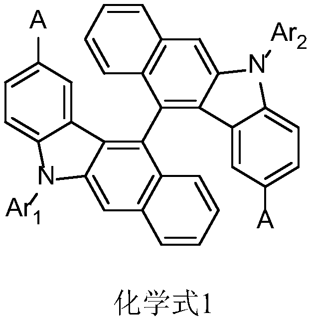
Figure 1 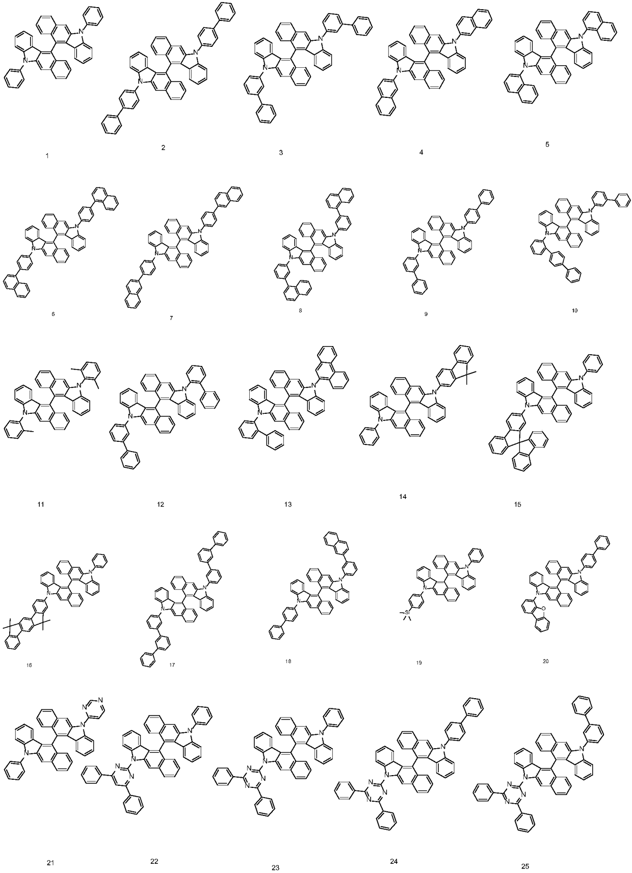
Figure 2 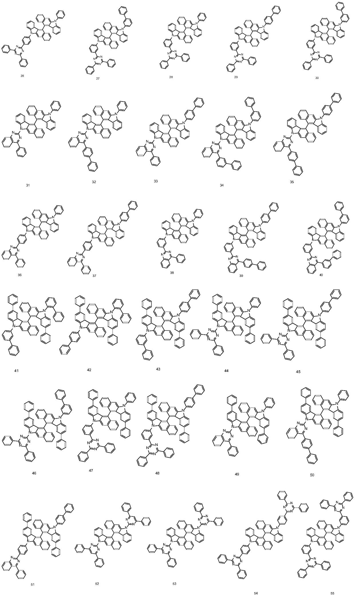
Figure 3
Abstract
Description
technical field
[0001] The invention relates to the technical field of luminescent materials, in particular to an organic electroluminescence material, a preparation method thereof and an organic electroluminescence device. Background technique
[0002] An electroluminescent device is a display device that uses electroluminescent materials to be excited to emit light. As a self-luminous display device, it has the advantages of wide viewing angle, good contrast, and fast response speed. In 1987, Kodak first developed an organic electroluminescent device (OLED) using low-molecular aromatic diamines and aluminum complexes as light-emitting layer materials.
[0003] OLED has the advantages of thin and light, active light emission, wide viewing angle, fast response, low energy consumption, excellent low temperature and shock resistance, and potential flexible design. OLED is an all-solid-state device with no vacuum cavity and no liquid components, so it is not afraid of vibratio...
Examples
Synthetic example
[0047] Synthesis of intermediate e:
[0048]
[0049] Compound a (21g, 52.6mmol) was dissolved in tetrahydrofuran (300mL), hexane solvent was added dropwise at -78°C, 2.5M n-butyllithium (25.2mL, 63.1mmol) was stirred for one hour. Trimethyl borate (18.2 mL, 79 mmol) was slowly added dropwise and then stirred for 2 h. After neutralization by dropwise addition of 2M hydrochloric acid, the product was extracted with ethyl acetate and water. Recrystallization from dichloromethane and hexane gave compound b (8.4 g, 47%).
[0050] Compound b (85.8 g, 251 mmol), compound c (50.7 g, 251 mmol), tetrakistriphenylphosphine palladium (11 g, 10 mmol) and potassium carbonate (84.2 g, 609 mmol) were dissolved in toluene (1 L) / EtOH (200 mL) / distilled water (200 mL) and then heated at 90° C. for 2 hours. The organic layer was triturated with methanol after distillation under reduced pressure. The obtained solid was dissolved in dichloromethane, filtered through silica gel, and tritura...
Embodiment 1
[0158] [Example 1] Green light organic electroluminescent device (phosphorescent host)
[0159] First, 60nm (N1,N1'-([1,1'-biphenyl]-4,4'-diyl)bis(N1-(naphthalen-1-yl)-N4,N4- diphenylbenzene-1,4-diamine) to form a hole injection layer. The above hole injection layer is vapor-deposited with N,N'-diphenyl-N,N'-(1-naphthyl)-1,1'-biphenyl- 4,4'-Diamine (NPD) 60nm, compound 1 of the present invention and doped Ir(ppy) 3 [Tris(2-phenylpyridine)iridium] 95:5 weight ratio evaporation 30nm, bis(2-methyl-8-hydroxyquinoline-N1,O8)-(1,1'-biphenyl-4- Hydroxy) aluminum (BAlq) hole blocking layer vapor deposition 10nm, vapor deposition electron transport layer 8-hydroxyquinoline aluminum (Alq 3 ) 40nm, evaporated LiF 0.2nm to form the electron injection layer, evaporated Al 150nm to form the cathode.
[0160] [Example 2]-[Example 42] Green light organic electroluminescent device
[0161] Green-light host material of the light-emitting layer Except that the compound described in Table 1 w...
Embodiment 43
[0171] [Example 43] Red photoelectron light-emitting device (phosphorescent host)
[0172] First, 2-TNATA was vapor-deposited on the ITO layer (anode) formed on the glass substrate to a thickness of 60nm to form a hole injection layer, and a hole-transport layer NPD was vapor-deposited on the hole injection layer to a thickness of 60nm. The compound 31 and the dopant substance (piq) of host material Table 2 are vapor-deposited on the hole transport layer 2 Ir(acac)[bis-(1-phenylisoquinolyl)iridium(III)acetylacetonate] / 95:5 weight ratio 30nm thickness, evaporated hole blocking layer BAlq 10nm thickness, evaporated electron transport layer Alq 3 40nm thickness, vapor-deposited electron injection layer LiF 0.2nm thickness, vapor-deposited Al 150nm thickness to form the cathode.