
Shield gate groove type field effect transistor with variable doping structure and preparation method of shield gate groove type field effect transistor
A field-effect transistor, shielded gate technology, applied in semiconductor/solid-state device manufacturing, semiconductor devices, electrical components, etc., can solve the problems of reducing specific on-resistance, inability to meet, and low impact on specific on-resistance, and achieve suppression Turn on, improve avalanche capability, effect of short channel length
Patent Information
- Authority / Receiving Office
- CN · China
- Patent Type
- Applications(China)
- Current Assignee / Owner
- Publication Date
- 2022-03-08
Smart Images
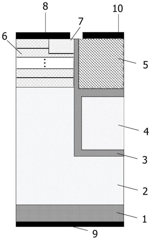
Figure 1 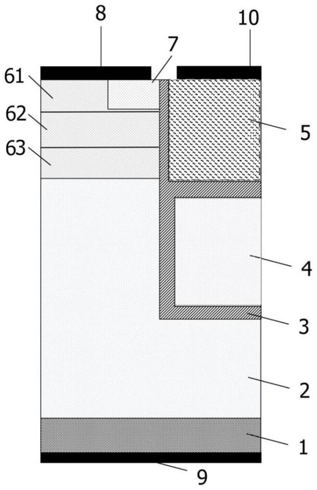
Figure 2 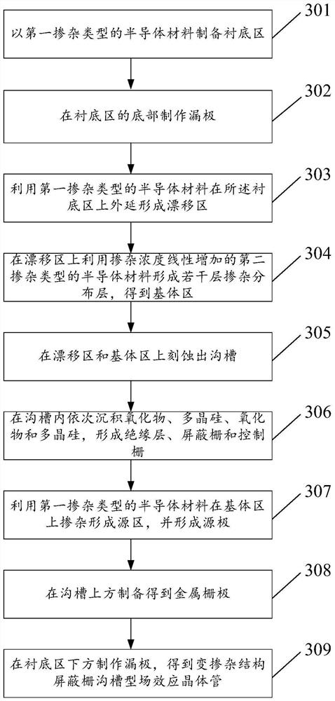
Figure 3
Abstract
Description
technical field
[0001] The present application relates to the field of semiconductor technology, in particular to a variable doping structure shielded gate trench type field effect transistor and a preparation method thereof. Background technique
[0002] Compared with the traditional trench transistor, the shielded gate trench field effect transistor has higher channel density and better charge compensation effect, and its shielded gate structure effectively reduces the transfer capacitance, so it has a lower ratio On-resistance, smaller conduction and switching losses, and higher operating frequency are widely used in important fields such as power management.
[0003] When the breakdown voltage is less than 300V, especially when the breakdown voltage is less than 100V, or even less than 40V, the channel region and the drift region have comparable specific on-resistance. Therefore, for low-voltage shielded gate trench type For field effect transistors, the improvement of ...
Examples
Embodiment 1
[0038] When the breakdown voltage is less than 300V, especially when the breakdown voltage is less than 100V, or even less than 40V, the channel region and the drift region have comparable specific on-resistance, and the structure improvement of the drift region has a significant impact on the breakdown voltage of the transistor. The improvement effect is obvious, but the influence on the specific on-resistance of the channel region is relatively low, and it cannot meet the requirement of lowering the specific on-resistance of shielded gate trench field effect transistors with low voltage levels.
[0039] In view of the above problems, an embodiment of the present application provides a shielded gate trench type field effect transistor with a variable doping structure, which can effectively reduce the specific on-resistance of the channel region.
[0040] The technical solutions of the embodiments of the present application are described in detail below with reference to the ac...
Embodiment 2
[0055] Based on the variable doping structure shielded gate trench type field effect transistor shown in the first embodiment above, the embodiment of the present application provides a variable doping structure shielded gate trench type field effect transistor with three doping distribution layers distributed at equal intervals. field effect transistor.
[0056] see figure 2 , the variable doping structure shielded gate trench field effect transistor, comprising: a substrate region 1, a drift region 2, a shielded gate 4, a control gate 5, a base region 6, a source region 7, an insulating layer 3, and a source 8 , drain 9 and metal gate 10;
[0057] Wherein, the drift region 2 , the base region 6 , the source region 7 and the source 8 are sequentially disposed above the substrate region 1 , and the drain 9 is disposed below the substrate region 1 , the control gate 5 and the shielding gate 4 are arranged on the same side of the drift region 2 from top to bottom, and the con...
Embodiment 3
[0066] Corresponding to the above embodiments of the shielded gate trench field effect transistor with variable doping structure, the present application also provides a method for manufacturing a shielded gate trench field effect transistor with variable doping structure and corresponding embodiments.
[0067] image 3 It is a schematic flowchart of a method for manufacturing a shielded gate trench field effect transistor with a variable doping structure shown in an embodiment of the present application.
[0068] see image 3 , the preparation method of the variable doping structure shielded gate trench type field effect transistor, comprising:
[0069] 301. Prepare a substrate region with a semiconductor material of the first doping type;
[0070] In the embodiment of the present application, the semiconductor material is a silicon material or a silicon carbide material. In step 301, the semiconductor material is an N-type heavily doped material, and its doping concentrat...