
Transfer-laminating member and production method thereof
Patent Information
- Authority / Receiving Office
- US · United States
- Current Assignee / Owner
- Publication Date
- 2005-06-23
- Estimated Expiration
- Not applicable · inactive patent
Smart Images
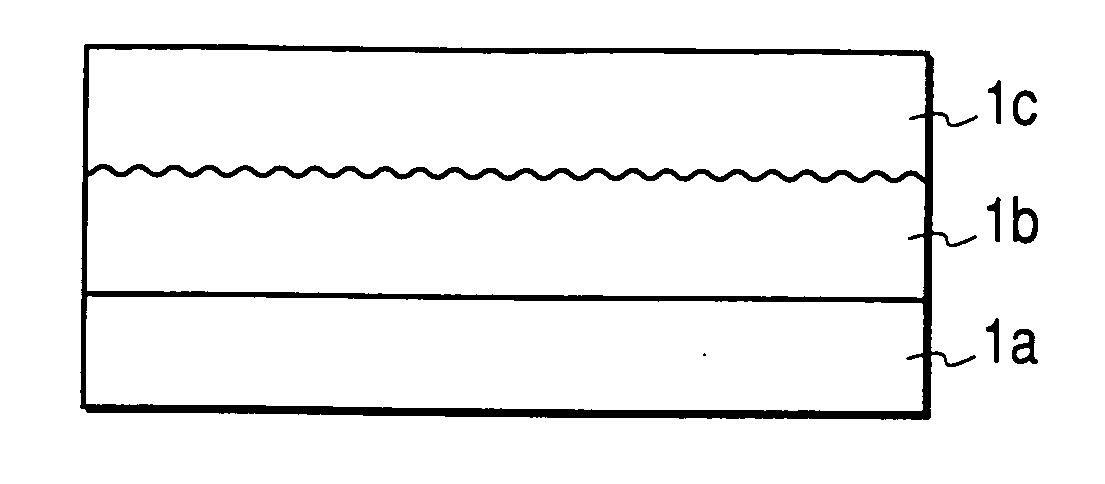
Figure 1 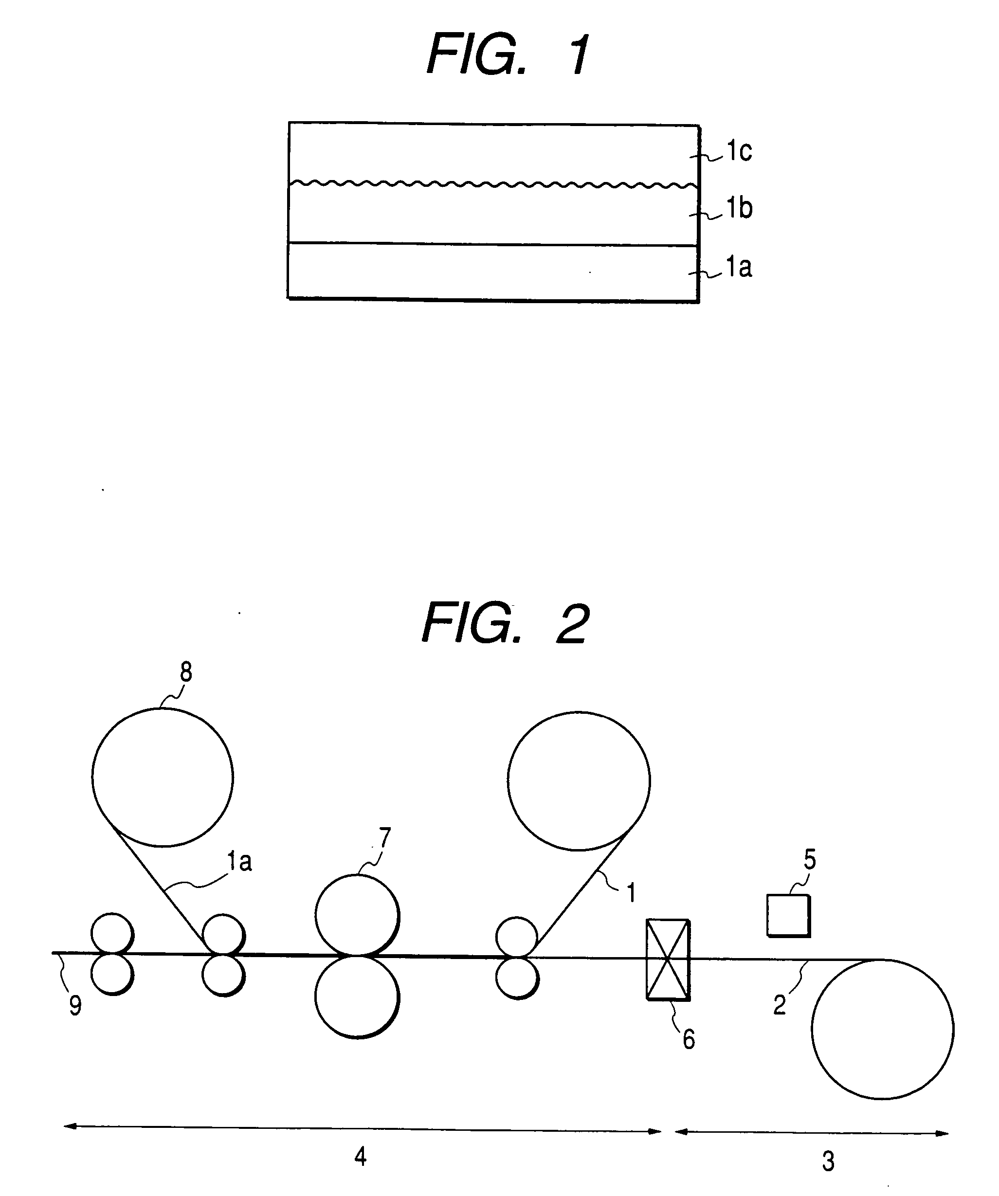
Figure 2
Abstract
Description
BACKGROUND OF THE INVENTION
[0001] 1. Field of the Invention
[0002] The present invention relates to a transfer-laminating member for forming minute irregularities to a transfer-receiving medium.
[0003] 2. Related Art
[0004] Printed articles by ink-jet, offset printing, gravure printing, electrophotography or the like are known to be improved in fastness properties of images, such as light fastness, water fastness and rub-off resistance, by transfer-laminating a surface-protecting layer on image-formed surfaces (image surfaces) thereof.
[0005] As a laminating member, is known a structure that a release layer and a protecting layer have been formed on a base material in that order. In order to improve the visibility of the images, it is known to mat the surface of the surface-protecting layer after transfer.
[0006] As methods for matting the surface of the surface-protecting layer, Japanese Patent Application Laid-Open No. 2001-105749 describes methods of causing various kinds of par...
Examples
example 1
[0034] One hundred parts by mass of SHC 900 (trade name, product of GE Toshiba Silicone Co., Ltd.; a mixed solution of a silicone resin, a melamine resin and an alkyd resin; solvent:metyl ethyl keton; solid content: 30%) were mixed with 3 parts by mass of Sylysia 256 (trade name, product of Fuji Silysia Chemical Co., Ltd.; silica gel; average particle diameter: 3.0 μm), and the resultant mixture was fully stirred to prepare a coating formulation for a release layer. The coating formulation for the release layer was applied on a polyethylene terephthalate film (film thickness: 25 μm) by a Wire bar so as to give a coating weight of 10 g / m2 and then dried at 100° C. for 1 minute to obtain a matt film.