
Conductive Material For Connecting Part And Method For Manufacturing The Conductive Material
Patent Information
- Authority / Receiving Office
- US · United States
- Current Assignee / Owner
- Publication Date
- 2008-04-17
Smart Images
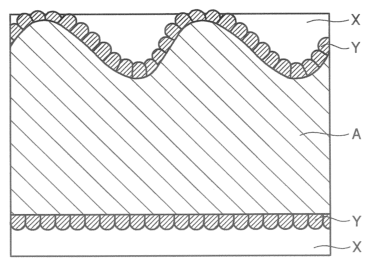
Figure 1 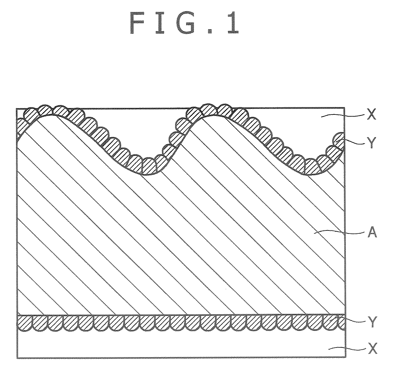
Figure 2 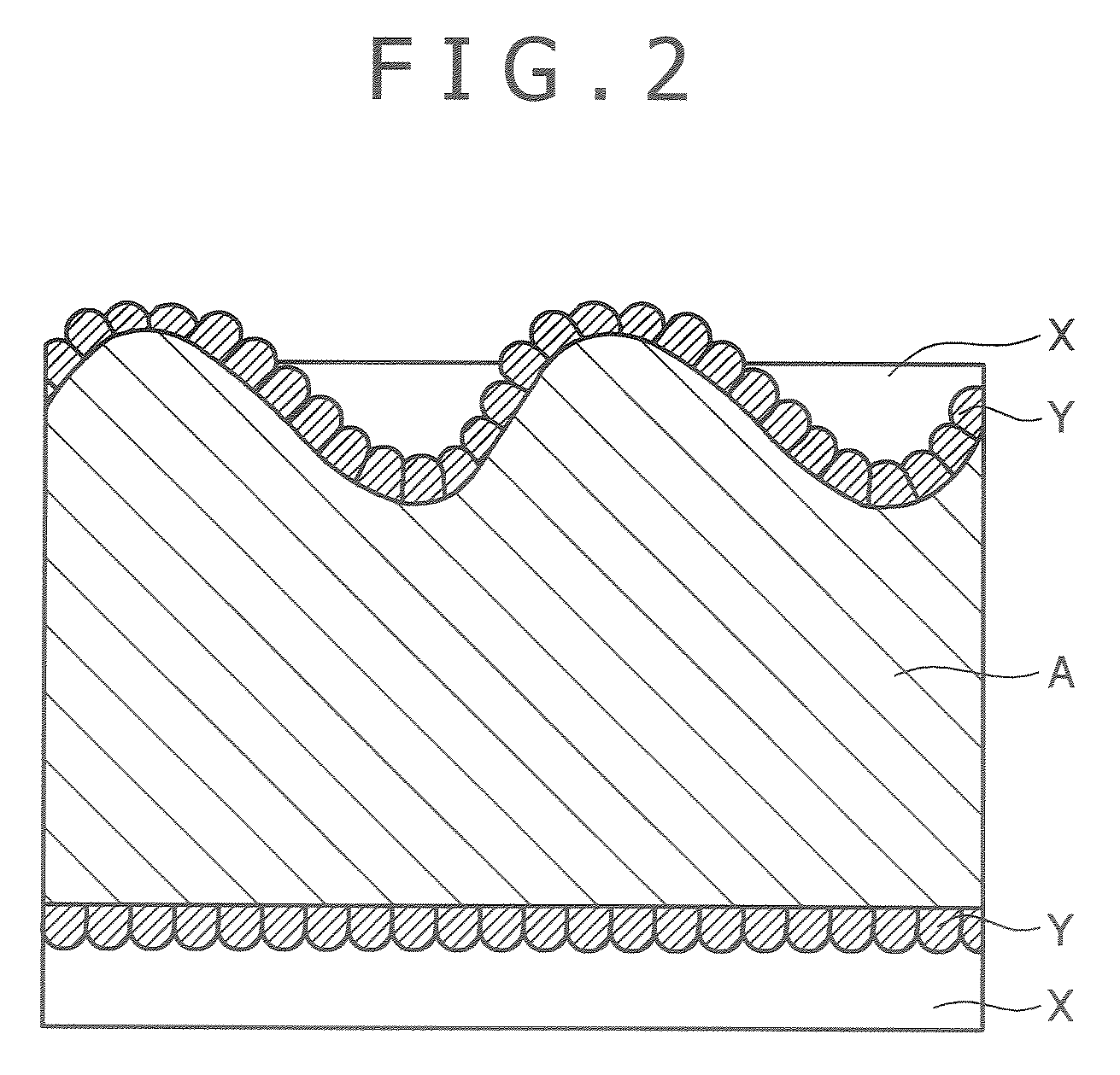
Figure 3
Abstract
Description
TECHNICAL FIELD
[0001] The present invention relates to a conductive material for a connecting part such as a connector terminal, bus bar, and so forth, used in electrical wiring mainly for automobiles, consumer equipment, and the like, and in particular, to a conductive material for a fitting type connecting part, of which reliability of electrical connection in applications as well as reduction in friction and wear upon insertion of a male form terminal into a female form terminal or pull-out of the former from the latter.BACKGROUND ART
[0002] For the conductive material for the connecting part such as the connector terminal, bus bar, and so forth, used in electrical wiring for automobiles, consumer equipment, and the like, use is made of Cu or a Cu-alloy, with Sn plating applied thereto, (including an Sn-alloy plating such as solder plating and so forth) except the case of an important electrical circuit requiring high reliability of electrical connection, against a low-level signal ...
Examples
embodiment 1
[Fabrication of Cu-Alloy Base Materials]
[0081]Table 1 snows chemical compositions of Cu-alloys (working examples Nos. 1, 2) used in the fabrication of Cu-alloy base materials. With the present embodiment, those Cu-alloys were subjected to surface roughening treatment by the mechanical method (rolling or polishing) to be finished into Cu-alloy base materials with a predetermined surface roughness, respectively, and having a thickness of 0.25 mm. The surface roughness was measured by the following procedure.
[Method for Measuring the Surface Roughness of the Cu-alloy Base Material]
[0082]The surface roughness of the Cu-alloy base material was measured on the basis of JIS B0601-1994 by use of a contact type surface-roughness tester (Surfcom 1400 model manufactured by Tokyo Seimitsu Co., Ltd.) The surface roughness was measured on a condition of a cutoff value at 0.8 mm, a reference length 0.8 mm, an evaluation length 4.0 mm, a measuring rate at 0.3 mm / s, and a stylus tip radius at 5 μm R...
embodiment 2
[0099]With respective test pieces, Cu plating was applied to a thickness of 0.15 μm to a base material made of the Cu-alloy No. 1, with the surface roughening treatment applied thereto, and further, Sn plating was applied thereto to respective thicknesses before the reflow process at 280° C. was applied for 10 seconds, thereby having obtained the test pieces (Nos. 11 to 19). Table 4 shows respective conditions under which those test pieces were fabricated. Among parameters for the surface roughness of the base material, the average interval Sm between the projections and the depressions was found in the preferable range as previously described (the range of 0.01 to 0.5 mm) with respect to all the test pieces. Further, the average thickness of the Cu plating layer, and that of the Sn plating layer, shown in Table 4, were measured by the same procedures as those described with reference to Embodiment 1.
TABLE 4Base MaterialArithmeticMeanNi platingCu PlatingSn PlatingTestRoughnessAverag...
embodiment 3
[0104]With respective test pieces, Cu plating was applied to a thickness of 0.15 μm to a base material made of the Cu-alloy No. 1, with the surface roughening treatment applied thereto, and further, Sn plating was applied thereto to respective thicknesses before the reflow process at 280° C. was applied for 10 seconds, thereby having obtained the test pieces (Nos. 20 to 25). Table 6 shows respective conditions under which the test pieces were fabricated. Among parameters for the surface roughness of the base material, the average interval Sm between the projections and depressions was found in the preferable range as previously described (the range of 0.1 to 0.5 mm) with respect to all the test pieces. Further, the average thickness of the Cu plating layer, and that of the Sn plating layer, shown in Table 6, were measured by the same procedures as those described with reference to Embodiment 1.
TABLE 6Base MaterialArithmeticMeanNi platingCu PlatingSn PlatingTestRoughnessAverageAverag...