
Sheet for Forming a Protective Film for Chips
Patent Information
- Authority / Receiving Office
- US · United States
- Current Assignee / Owner
- Publication Date
- 2009-02-26
- Estimated Expiration
- Not applicable · inactive patent
Smart Images
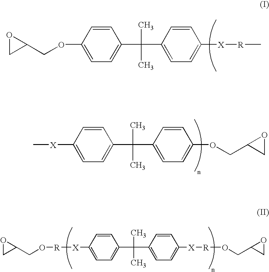
Figure 1 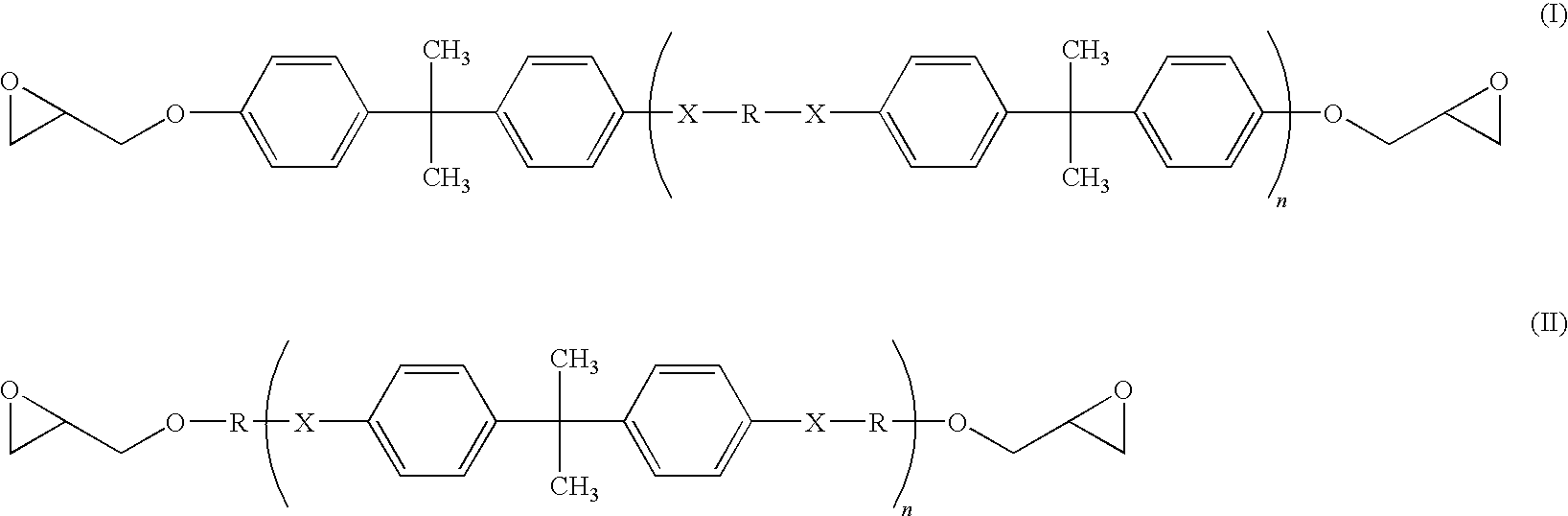
Figure 2 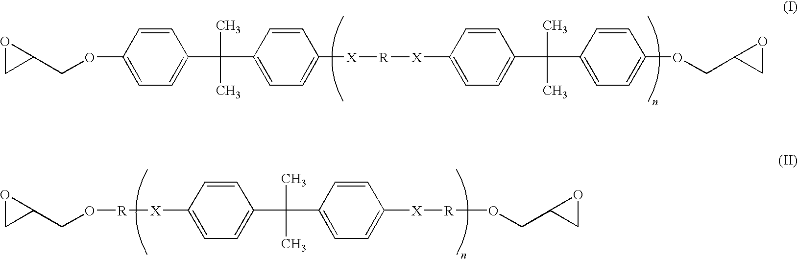
Figure 3
Abstract
Description
TECHNICAL FIELD
[0001] The present invention relates to a sheet for forming a protective film for chips, which is used to form a protective film on the back surface of such a chip as a semiconductor chip.BACKGROUND ART
[0002] In recent years, production of a semiconductor device by use of a so-called face down mounting process is being carried out. In the face down process, there is used a chip which has a convex portion called a bump on the circuit face side in order to secure electrical continuity and is connected to the substrate through the convex portion of the circuit face side.
[0003] Such semiconductor devices are generally produced though the following steps:
[0004] (1) forming a circuit on a surface of a semiconductor wafer by etching or the like and providing a bump on the appointed position of the circuit surface;
[0005] (2) grinding the back surface of semiconductor wafer to have a given thickness;
[0006] (3) fixing the back surface of semiconductor wafer onto a dicing sheet which ...
Examples
examples
[0066]Hereafter, the present invention will be described with reference to examples. However, the present invention is not limited to these examples.
[0067]The binder polymer, the epoxy resins, the fillers, and other components are shown below.
A: Binder Polymer
[0068]Acrylic polymer (copolymer of 55 parts by weight of butyl acrylate, 15 parts by weight of methyl methacrylate, 20 parts by weight of glycidyl methacrylate, and 15 parts by weight of 2-hydroxyethyl acrylate; weight average molecular weight, 900,000; glass transition temperature, −28° C.)
B: Epoxy Resin
[0069]B1: liquid bisphenol A type epoxy resin (molecular weight, ca. 370; epoxy equivalent, 180 to 200 g / eq)
[0070]B2: solid bisphenol A type epoxy resin (molecular weight, ca. 1,600; epoxy equivalent, 800 to 900 g / eq)
[0071]B3: dicyclopentadiene type epoxy resin (produced by DIC Corporation; trade name, Epiclon HP-7200HH)
[0072]B4: epoxy resin containing an ethylene glycol chain (produced by DIC Corporation; trade name, Epiclon ...
examples 1 to 3
, Comparative Examples 1 to 3
[0081]Each composition shown in Table 1 below and prepared using the materials described above was coated on the release treated surface of a polyethylene terephthalate film, one side of which is release treated (produced by Lintec Corporation; trade name, SP-PET 3811; thickness, 38 μm; surface tension, less than 30 mN / m; melting point, 200° C. or higher), in such a way that the thickness after removal of the solvent became 50 μm, followed by drying at 100° C. for 1 minute to afford the sheet for forming a protective film for chips.
[0082]The Evaluations were made. The results are shown in Table 1.
TABLE 1Comp.Comp.Comp.Example 1Example 2Example 3Ex. 1Ex. 2Ex. 3A117.6117.6105.3117.6117.6117.6B10.00.00.058.80.00.0B211.811.810.511.870.611.8B329.429.40.029.429.429.4B458.80.089.50.00.058.8B50.058.80.00.00.00.0B Total100100100100100100C352.9352.9352.9352.9352.90D12.92.92.62.92.92.9D22.92.92.62.92.92.9E11.811.810.511.811.811.8Warpage of0.50.80.25.84.60.7wafer (m...