
Interposer, module, and electronics device including the same
a technology of electronics device and module, applied in the direction of electrical apparatus construction details, semiconductor/solid-state device details, high-frequency circuit adaptations, etc., can solve the problems complicated antenna section and semiconductor chip section, etc., and achieve the effect of lowering reliability and yield ratio
Patent Information
- Authority / Receiving Office
- US · United States
- Patent Type
- Applications(United States)
- Current Assignee / Owner
- Publication Date
- 2011-02-10
- Estimated Expiration
- Not applicable · inactive patent
Smart Images
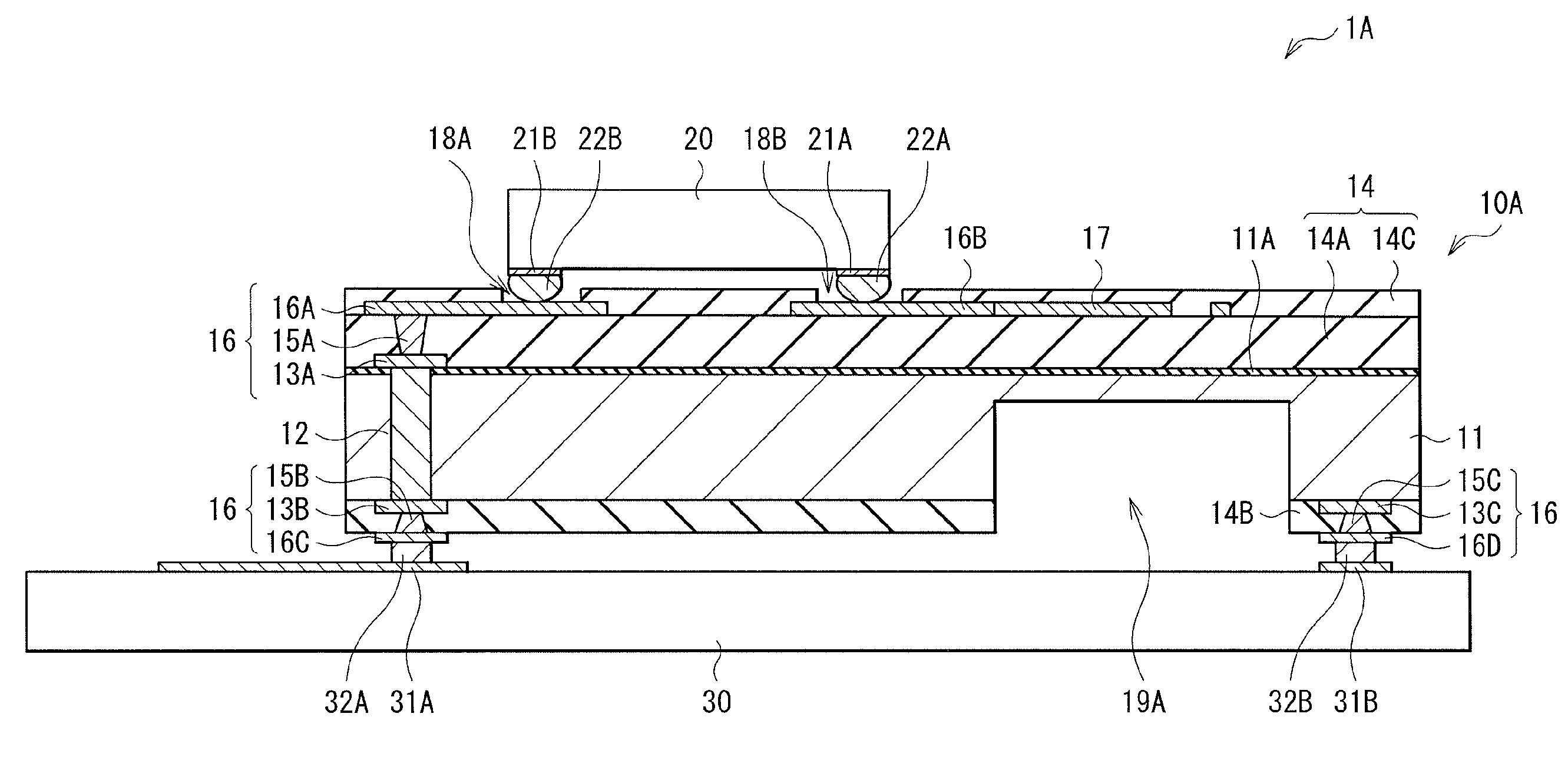
Figure 1 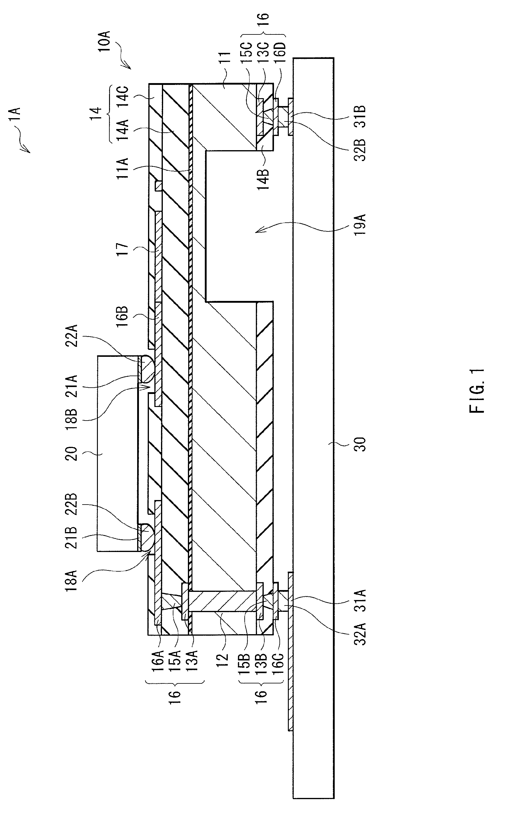
Figure 2 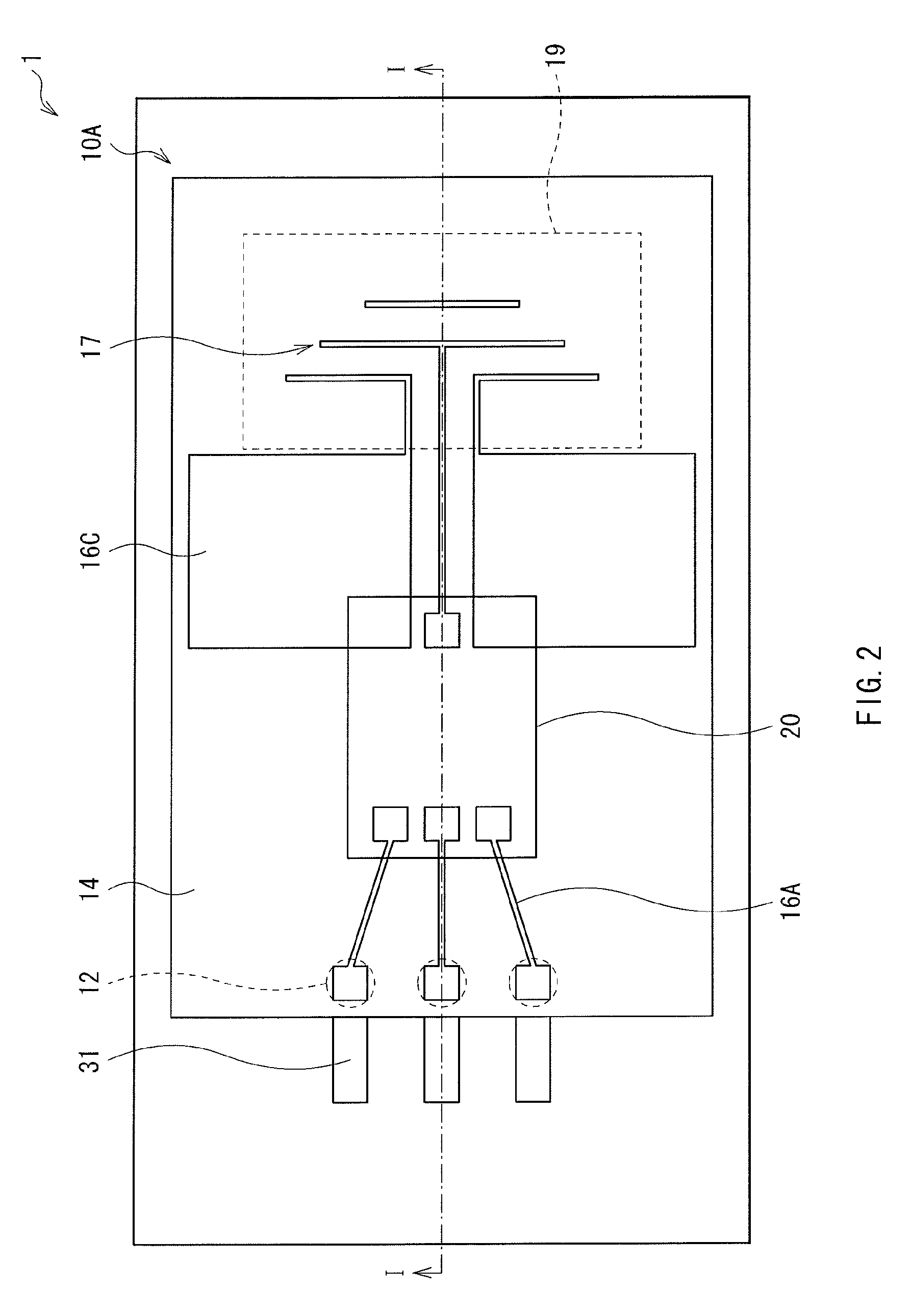
Figure 3
Abstract
Description
BACKGROUND OF THE INVENTION
[0001] 1. Field of the Invention
[0002] The present invention relates to an interposer for intermediating electric connection and mechanical connection among a plurality of electronic devices with each wiring rule different from each other, a module, and an electronics device including the same.
[0003] 2. Description of the Related Art
[0004] There is a single-digit or more gap between a pad pitch of a semiconductor chip whose miniaturization has been rapidly improved and a pad pitch of a substrate (mount substrate) on which the semiconductor chip is mounted. Such a gap leads to difficulty to reflect high performance obtained by progress of semiconductor technology and performance of a high function chip to a device or a system. For example, the practically used pad pitch of the semiconductor chip has been improved to 50 μm or less, while the pad pitch of the mount substrate (for example, a Print Circuit Board (PCB)) is about 500 μm. It is expected that miniaturi...
Examples
modified example
[0062]Next, a description will be given of an interposer 10C (10D) and a module 2A (2B) including the same according to a modified example of the interposer 10A (10B) and the module 1A (1B) including the same according to the foregoing embodiment. FIG. 11 illustrates a cross sectional structure of the module 2A including the interposer 10C having the concave section 19A in the substrate 11, and FIG. 12 illustrates a planar structure thereof FIG. 13 illustrates a cross sectional structure of the module 2B including the interposer 10D having the aperture 19B in the substrate 11. FIG. 11 and FIG. 13 are a cross sectional structure taken along line II-II of FIG. 12. For the same elements as those of the first embodiment, the same referential symbols are affixed thereto and the descriptions thereof will be omitted.
[0063]The interposer 10C (10D) connects the wiring layer 16 to the printed board 30 with a wiring 33. On the substrate 11, a chip-use connection section 23 is provided together...
application example
[0065]Next, a description will be given with reference to FIG. 14 of a configuration of a communication apparatus in which the interposer 10A of the embodiment of the invention is used. FIG. 14 illustrates a block configuration of the communication apparatus as an electronics device.
[0066]Examples of the communication apparatus illustrated in FIG. 14 include a mobile phone, a personal digital assistant (PDA), and a wireless LAN apparatus. For example, as illustrated in FIG. 14, the communication apparatus includes a transmission circuit 300A (module), a receiving circuit 300B (module), a transmitting / receiving switch 301 for switching the transmitting / receiving route, a high frequency filter 302, and a transmitting / receiving antenna 303.
[0067]The transmission circuit 300A includes two digital / analog converters (DAC) 311I and 311Q, and two bandpass filters 312I and 312Q that respectively correspond to transmission data of I channel and transmission data of Q channel, a modulator 320,...