
Method for fabricating semiconductor device
a semiconductor device and manufacturing method technology, applied in semiconductor devices, semiconductor/solid-state device details, electrical devices, etc., can solve the problems of oxidation or damage of the cap film b>7/b>, above-mentioned conventional techniques, etc., and achieve the effect of sufficiently reducing the capacitance between the wires
Patent Information
- Authority / Receiving Office
- US · United States
- Patent Type
- Patents(United States)
- Current Assignee / Owner
- Publication Date
- 2010-06-22
- Estimated Expiration
- Not applicable · inactive patent
Smart Images
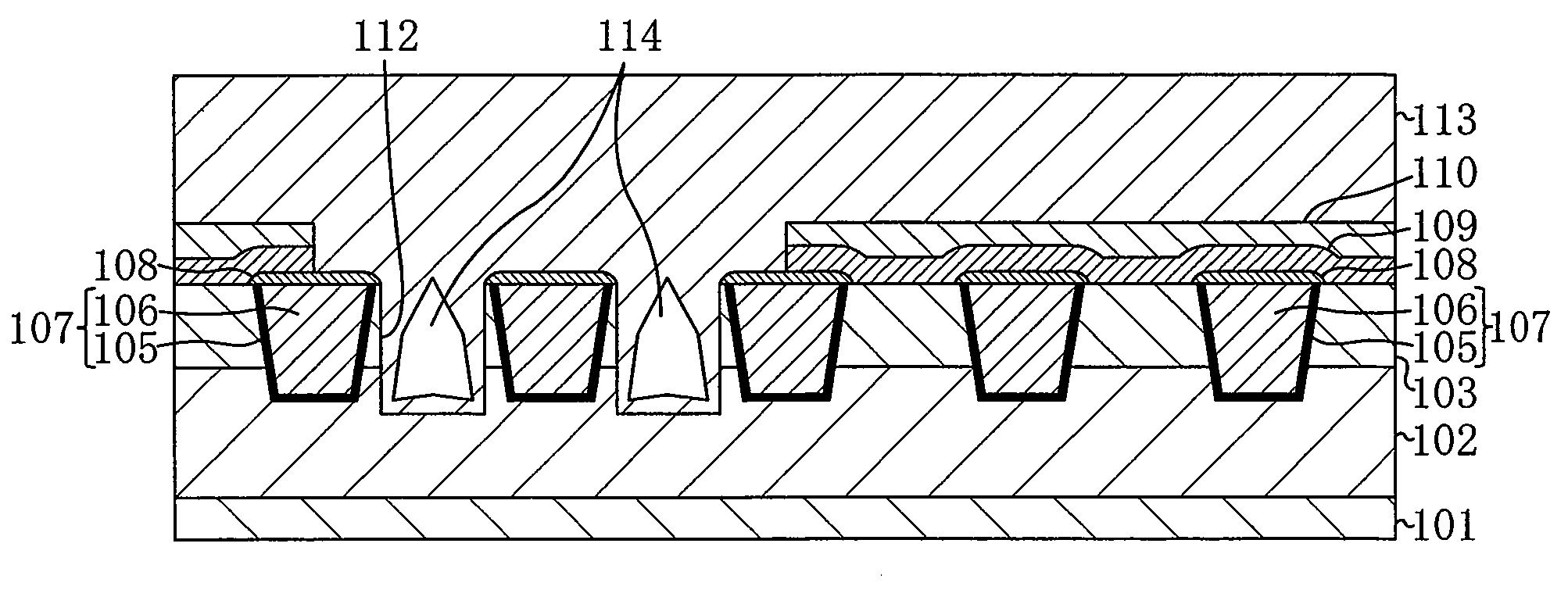
Figure 1 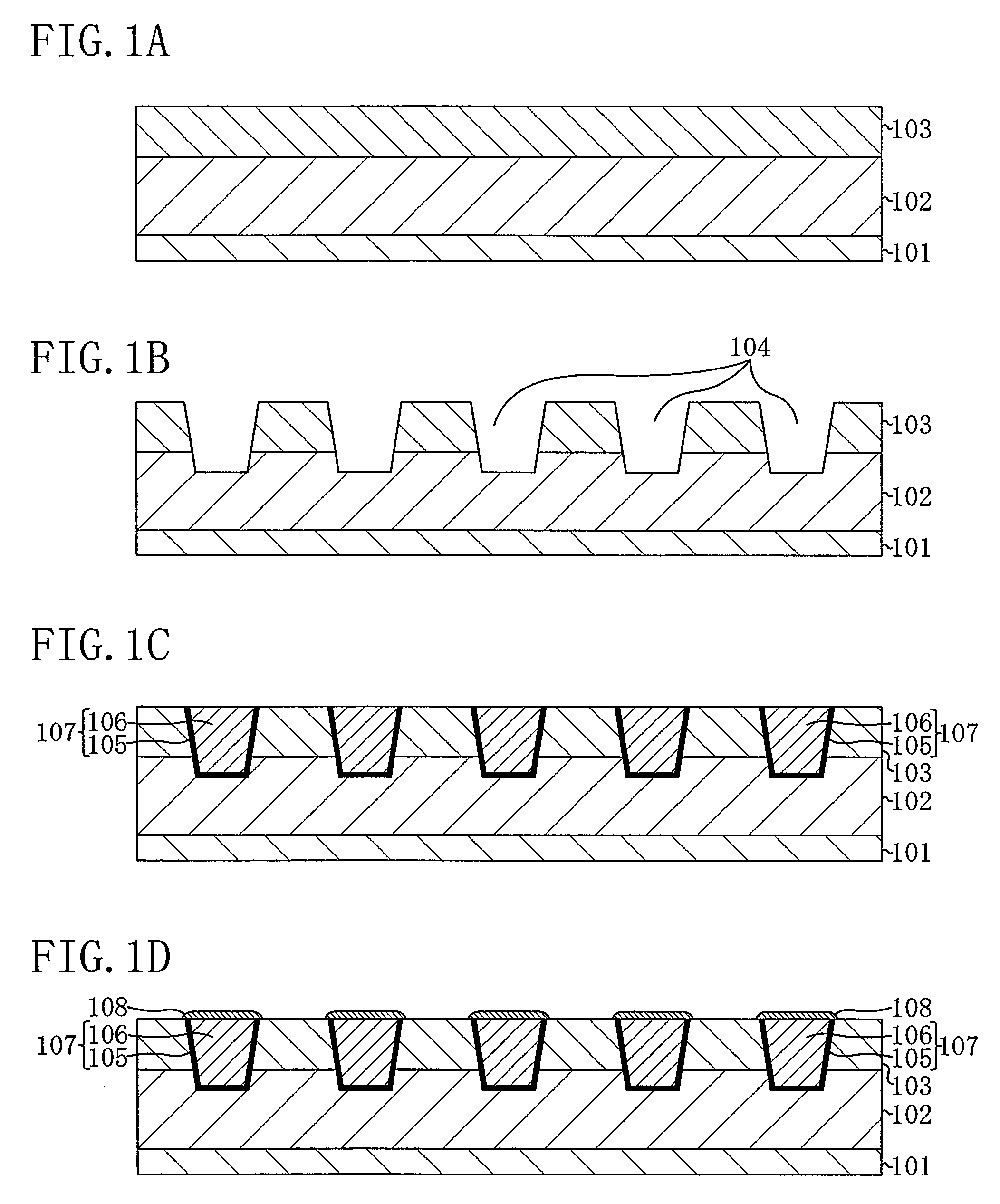
Figure 2 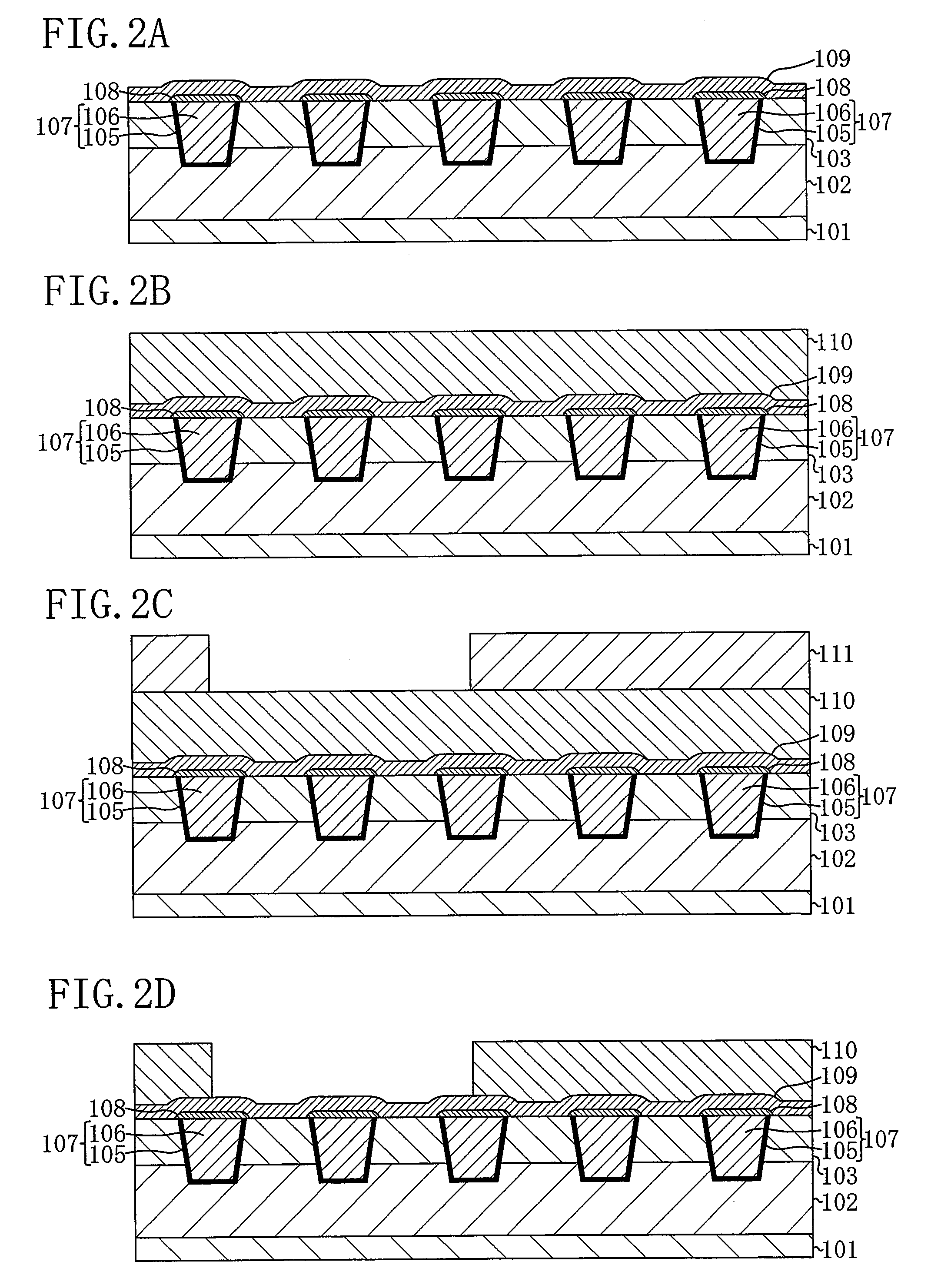
Figure 3
Abstract
Description
BACKGROUND OF THE INVENTION
[0001] 1. Field of the Invention
[0002] The present invention relates to a method for fabricating a semiconductor device.
[0003] 2. Description of the Prior Art
[0004] Progressing miniaturization of semiconductor integrated circuit device in recent years narrows a wire-to-wire spacing. This results in a problem that capacitance between wires increases, lowering the propagation velocity of a signal. To reduce the capacitance between the wires, it has been studied to embed an insulating film material having a low dielectric constant between the wires. Meanwhile, it has also been studied to form an air gap between the wires to reduce the capacitance between the wires. A conventional method for forming the air gap disclosed in Patent Document 1 will be described below with reference to the drawings.
[0005] First, as illustrated with FIG. 5A, on a surface of a semiconductor substrate 1, an insulating film 2 is formed.
[0006] Then, as illustrated with FIG. 5B, photolithogr...
Examples
embodiment 1
[0033]A method for fabricating a semiconductor device according to Embodiment 1 of the present invention will be described below with reference to the drawings.
[0034]FIGS. 1A through 1D, FIGS. 2A through 2D, and FIGS. 3A through 3D are cross-sectional views illustrating respective steps in the method for fabricating the semiconductor device according to Embodiment 1.
[0035]First, as illustrated with FIG. 1A, over a semiconductor substrate 101, an inter-layer insulating film 102 and an inter-wire insulating film 103 are formed. It is to be noted that in the present embodiment, as the inter-layer insulating film 102, for example, a SiOC film is used, and as the inter-wire insulating film 103, for example, a TEOS (tetraethylorthosilicate) film is used.
[0036]Then, as illustrated with FIG. 1B, photolithography and dry etching are performed to form wiring grooves 104 which penetrate through the inter-wire insulating film 103 and reach inside the inter-layer insulating film 102.
[0037]Then, ...
embodiment 2
[0058]A method for fabricating a semiconductor device according to Embodiment 2 of the present invention will be described below with reference to the drawings. It is to be noted that descriptions as to Embodiment 2 are given of only different points from Embodiment 1 described above, and the same descriptions as those of Embodiment 1 are not repeated.
[0059]FIG. 4A is a cross-sectional view illustrating a step of the method for fabricating the semiconductor device according to Embodiment 2. The present embodiment is different from Embodiment 1 in that between the step of forming the air gap grooves 112 of FIG. 3C and the step of forming the air gaps 114 of FIG. 3D (the step of forming the inter-layer insulating film 113), the hard mask film 110 is removed by wet etching or the like as illustrated with FIG. 4A. This makes it possible to directly deposit the inter-layer insulating film 113 on the protection film 109 in the step of forming the air gaps 114 of FIG. 3D. Therefore, it is ...