
Direct drive waveform generator
a generator and drive technology, applied in the direction of pulse generator, pulse manipulation, pulse technique, etc., can solve the problems of reducing efficiency, manufacturing devices, and difficult to deal with high voltage, and achieve the effect of eliminating high voltage amplifiers
Patent Information
- Authority / Receiving Office
- US · United States
- Patent Type
- Applications(United States)
- Current Assignee / Owner
- Publication Date
- 2012-12-13
- Estimated Expiration
- Not applicable · inactive patent
Smart Images
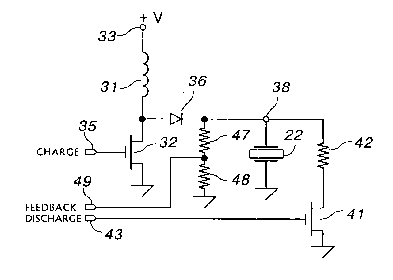
Figure 1 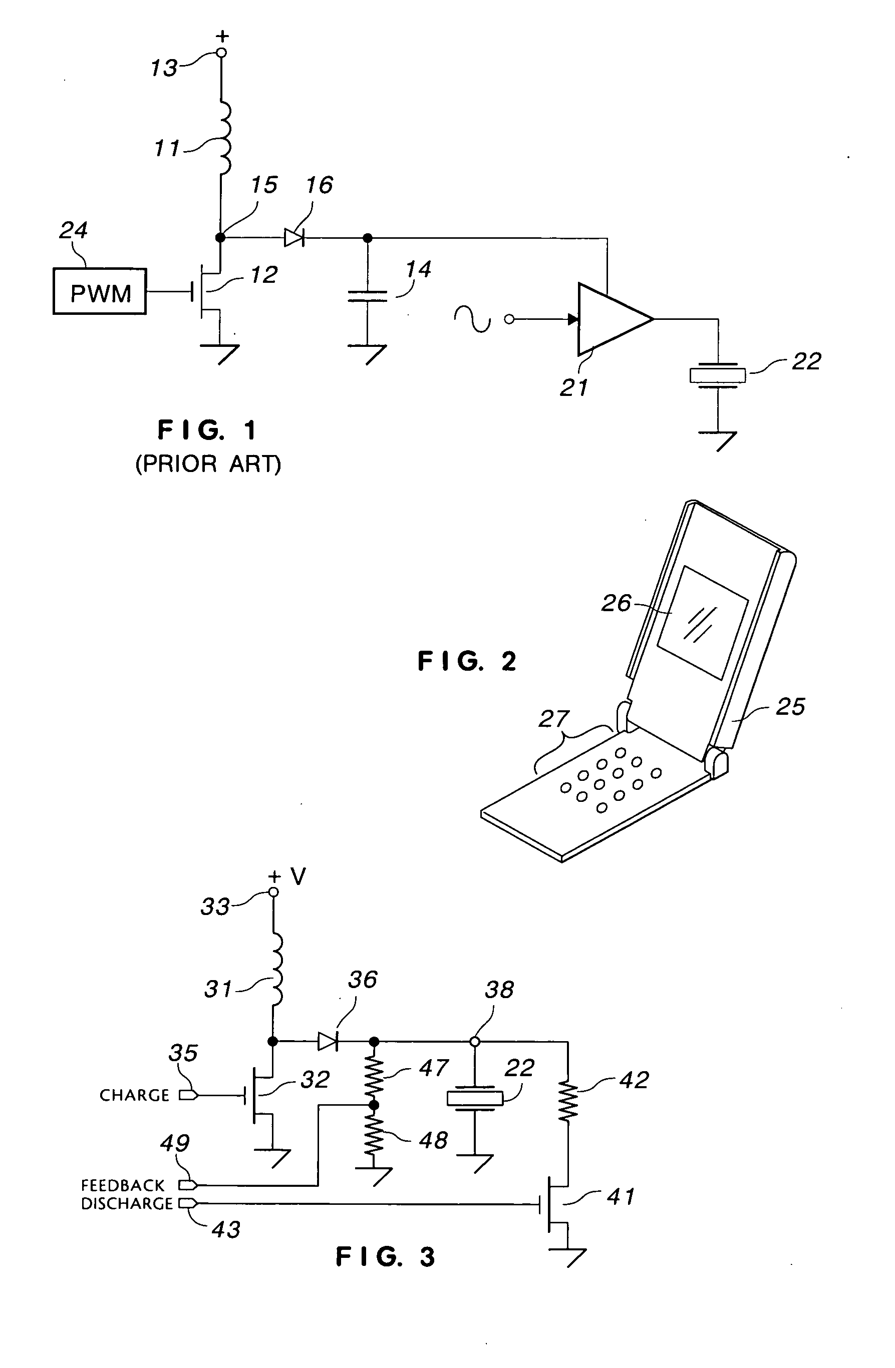
Figure 2 
Figure 3
Abstract
Description
[0001] This invention relates to a battery powered driver and, in particular, to a driver for piezoelectric devices that drives a device by creating a high voltage waveform similar to a low voltage control signal and applying the waveform directly to the piezoelectric device.BACKGROUND
[0002] A piezoelectric actuator requires high voltage, greater than typical battery voltages of 1.5 to 12.6 volts. A “high” voltage is 20-200 volts, with 100-120 volts currently being a typical drive voltage. Some line driven power supplies for actuators provide as much as 1000 volts. Producing high voltage from a battery is more difficult than producing high voltage from a power line.
[0003] A voltage boost converter can be used to convert the low voltage from a battery to a higher voltage for the driver. In a boost converter, the energy stored in an inductor is supplied to a capacitor as pulses of current at high voltage.
[0004] FIG. 1 is a schematic of a circuit including a known boost converter; e.g. see...
Examples
Embodiment Construction
[0028]FIG. 2 illustrates electronic device 25 including display 26 and keypad 27. Either the display or the keypad, or both, can be provided with a piezoelectric device (not shown in FIG. 2) for providing tactile feedback when a key or a portion of the display is depressed slightly. Devices for providing feedback are known in the art. As described above, such devices can be single layer or have plural layers and be unidirectional or bi-directional.
[0029]FIG. 3 is a block diagram of a preferred embodiment of the invention that eliminates storage capacitor 14 (FIG. 1) and high voltage amplifier 21 (FIG. 1). Inductor 31 and transistor 32 are connected in series between supply 33 and ground or common. The control terminal of transistor 32 is coupled to CHARGE input 35. The junction of inductor 31 and transistor 32 is coupled by diode 36 to output terminal 38. Piezoelectric actuator 22 is coupled between output terminal 38 and ground. The circuit describes thus far is a charging circuit ...