
Land grid array connector assembly with reliable block
a technology of connectors and blocks, applied in the field of electrical connectors, can solve the problems of easy damage to the sidewall, difficult to ensure reliable signal transmission between the terminals and the lga chip,
Patent Information
- Authority / Receiving Office
- US · United States
- Patent Type
- Patents(United States)
- Current Assignee / Owner
- Publication Date
- 2005-08-16
- Estimated Expiration
- Not applicable · inactive patent
Smart Images
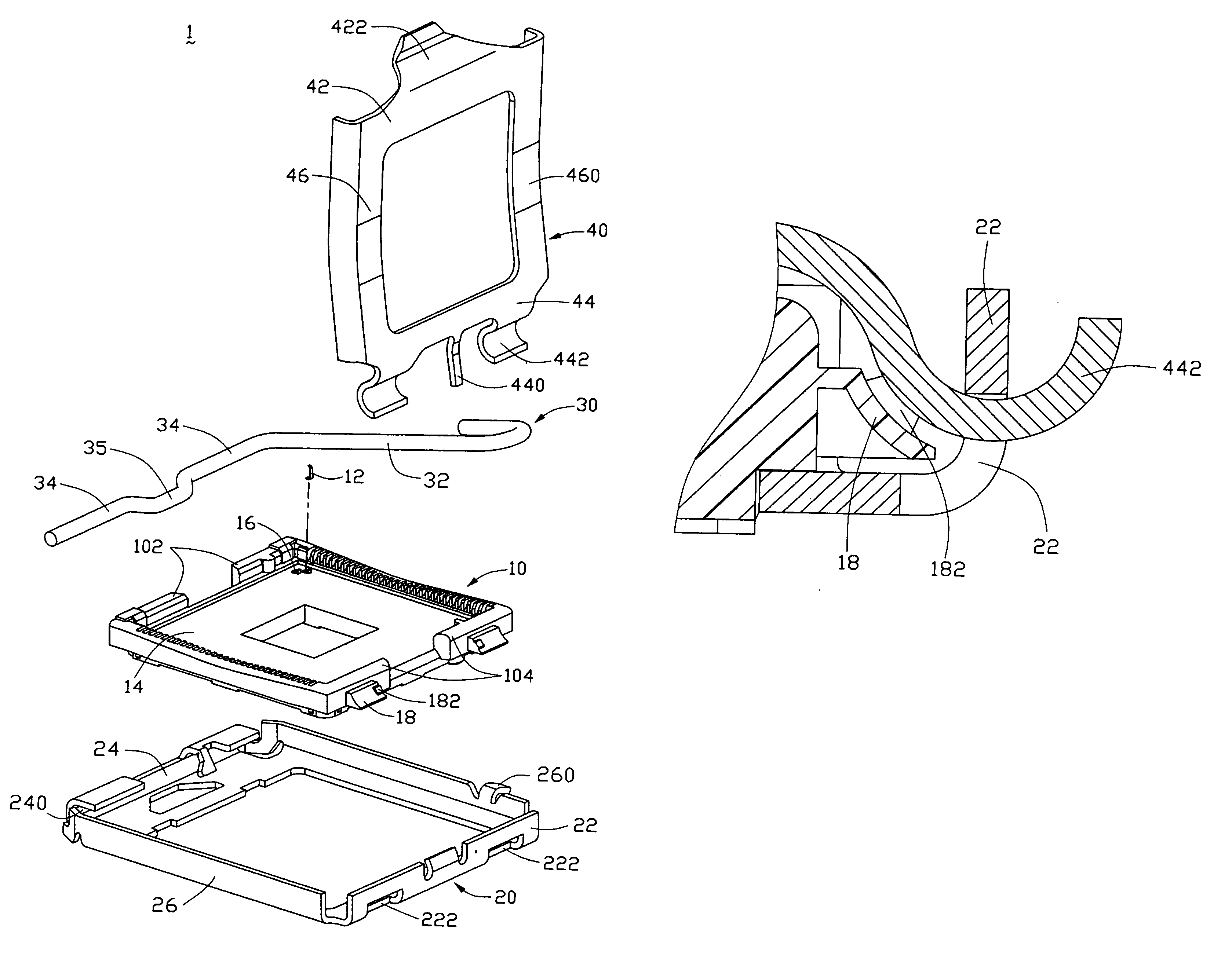
Figure 1 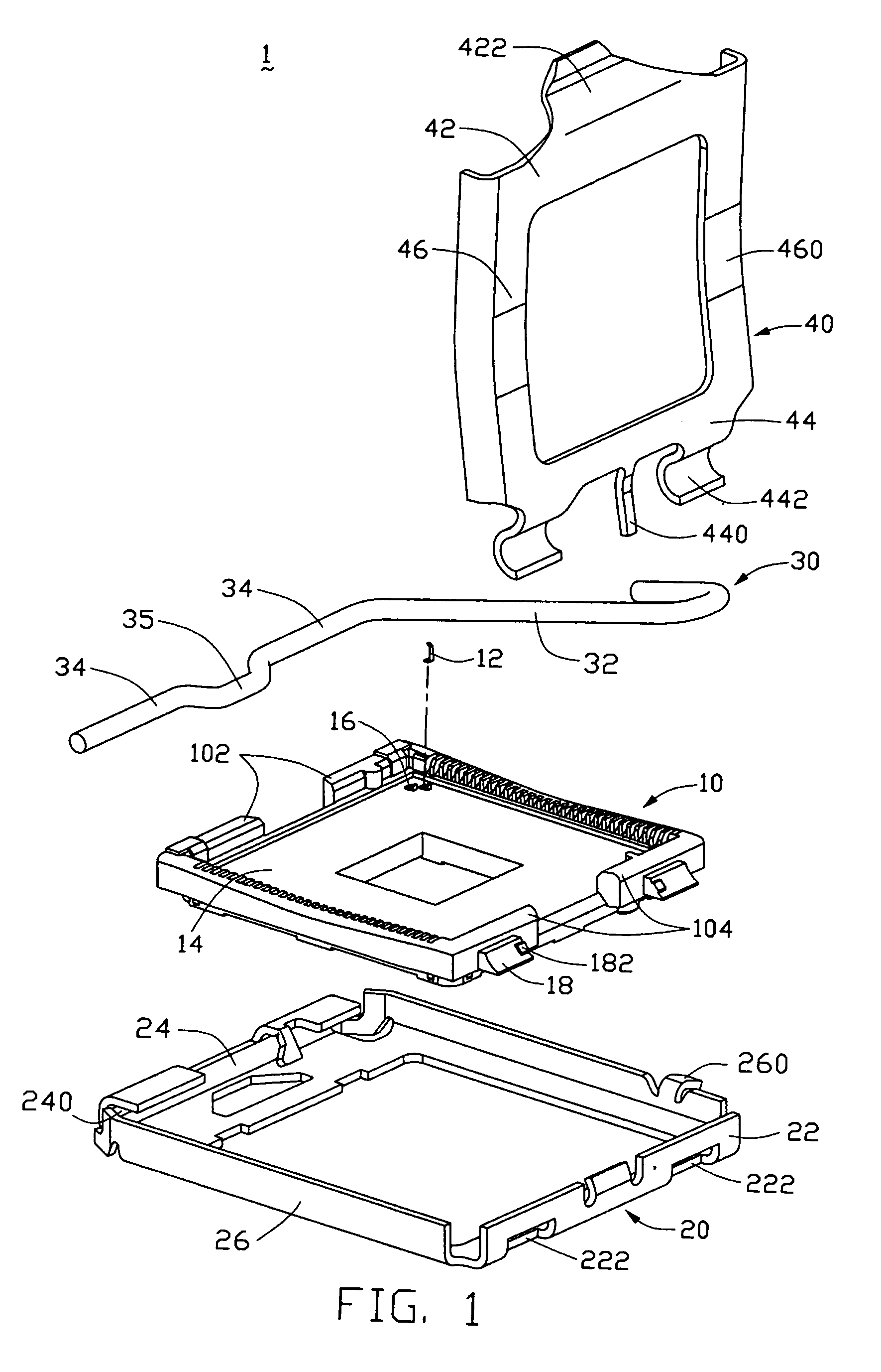
Figure 2 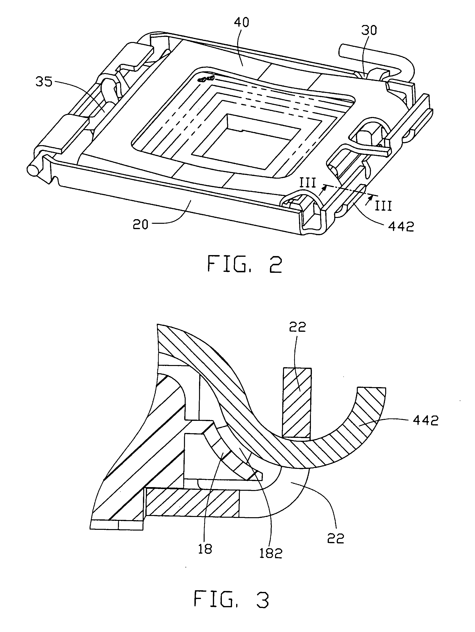
Figure 3
Abstract
Description
BACKGROUND OF THE INVENTION
[0001] 1. Field of the Invention
[0002] The present invention relates to the art of electrical connectors, and more particularly to a land grid array (LGA) connector assembly provided for mechanically and electrically connecting a land grid array (LGA) chip to a printed circuit board (PCB).
[0003] 2. Description of the Prior Art
[0004] Land grid array (LGA) electrical connectors are widely used in the connector industry for electrically connecting LGA chips to printed circuit boards (PCBs) in personal computers (PCs). Conventionally, an LGA connector mainly comprises an insulative housing, a multiplicity of terminals received therein, a load plate and a cam lever pivotably mounted on two opposite sides of the housing. The housing defines a multiplicity of terminal passageways in a rectangular array, for interferentially receiving corresponding terminals. Due to the very high density of leads arranged on an LGA chip, the LGA chip needs to be precisely seated on th...
Examples
Embodiment Construction
[0020]Reference will now be made to the drawings to describe the present invention in detail.
[0021]FIG. 1 is an exploded, isometric view of a land grid array (LGA) connector assembly 1 in accordance with a preferred embodiment of the present invention. The LGA connector assembly 1 provided for electrically connecting an LGA chip (not shown) to a PCB (not shown) includes an a generally rectangular insulative housing 10, a multiplicity of terminals 12 received in the housing 10, a metal stiffener 20 partly covering and reinforcing the housing 10, a cam lever 30 pivotably attached to an end of the stiffener 20, and a metal clip 40 pivotably mounted to an opposite end of the stiffener 20 for engaging with the cam lever 30.
[0022]The housing 10 includes a first sidewall 102, a second sidewall 104 opposite to the first sidewall 102 and two opposite third sidewalls 106 adjacent the first and second sidewalls 102, 104 respectively. The four sidewalls cooperatively define a generally rectangu...