
Semiconductor storage device
a technology of semiconductors and storage devices, applied in the direction of digital storage, electronic circuit testing, instruments, etc., can solve the problems of complex testing operations, and achieve the effect of improving testability
Patent Information
- Authority / Receiving Office
- US · United States
- Patent Type
- Patents(United States)
- Current Assignee / Owner
- Publication Date
- 2007-07-03
- Estimated Expiration
- Not applicable · inactive patent
Smart Images
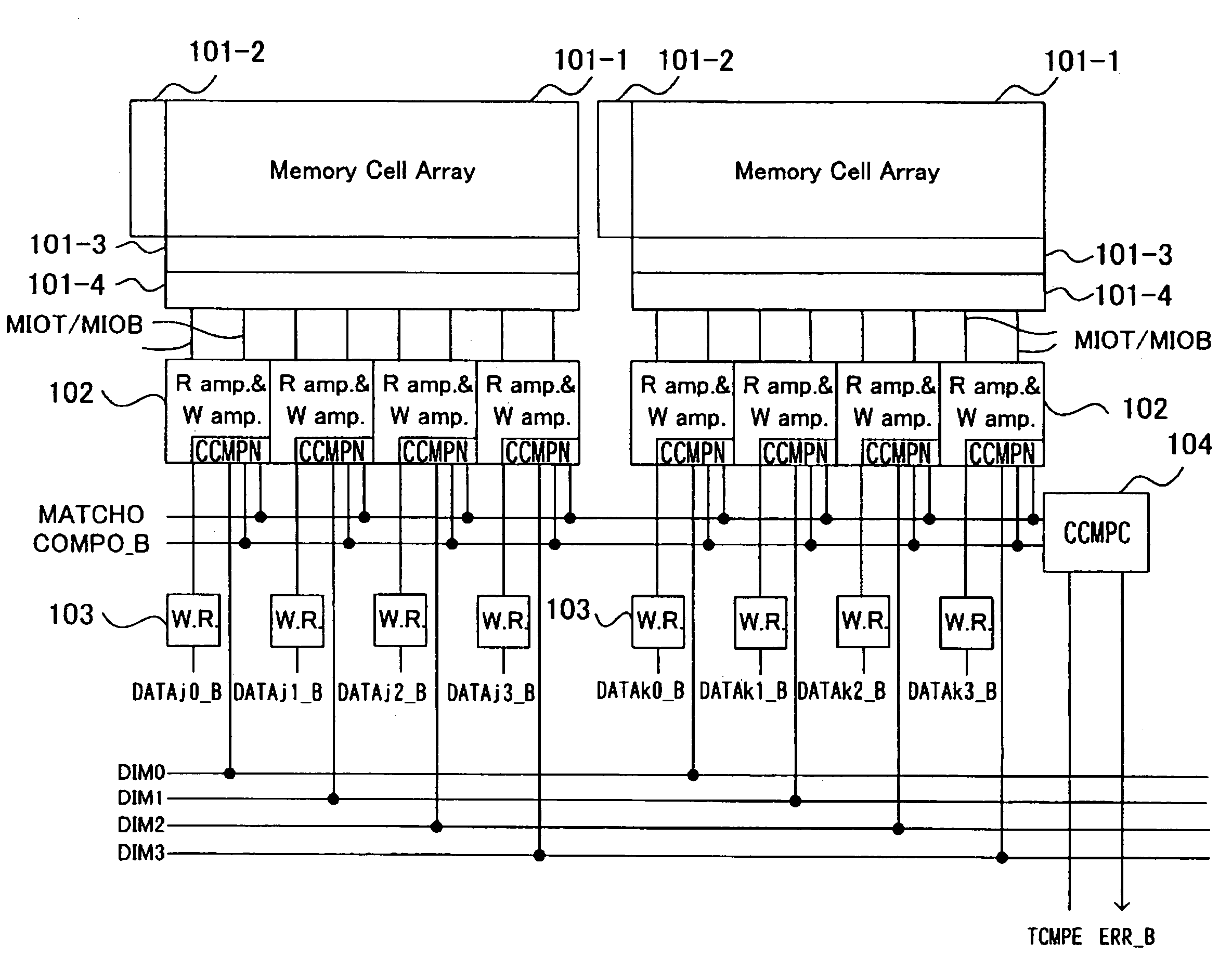
Figure 1 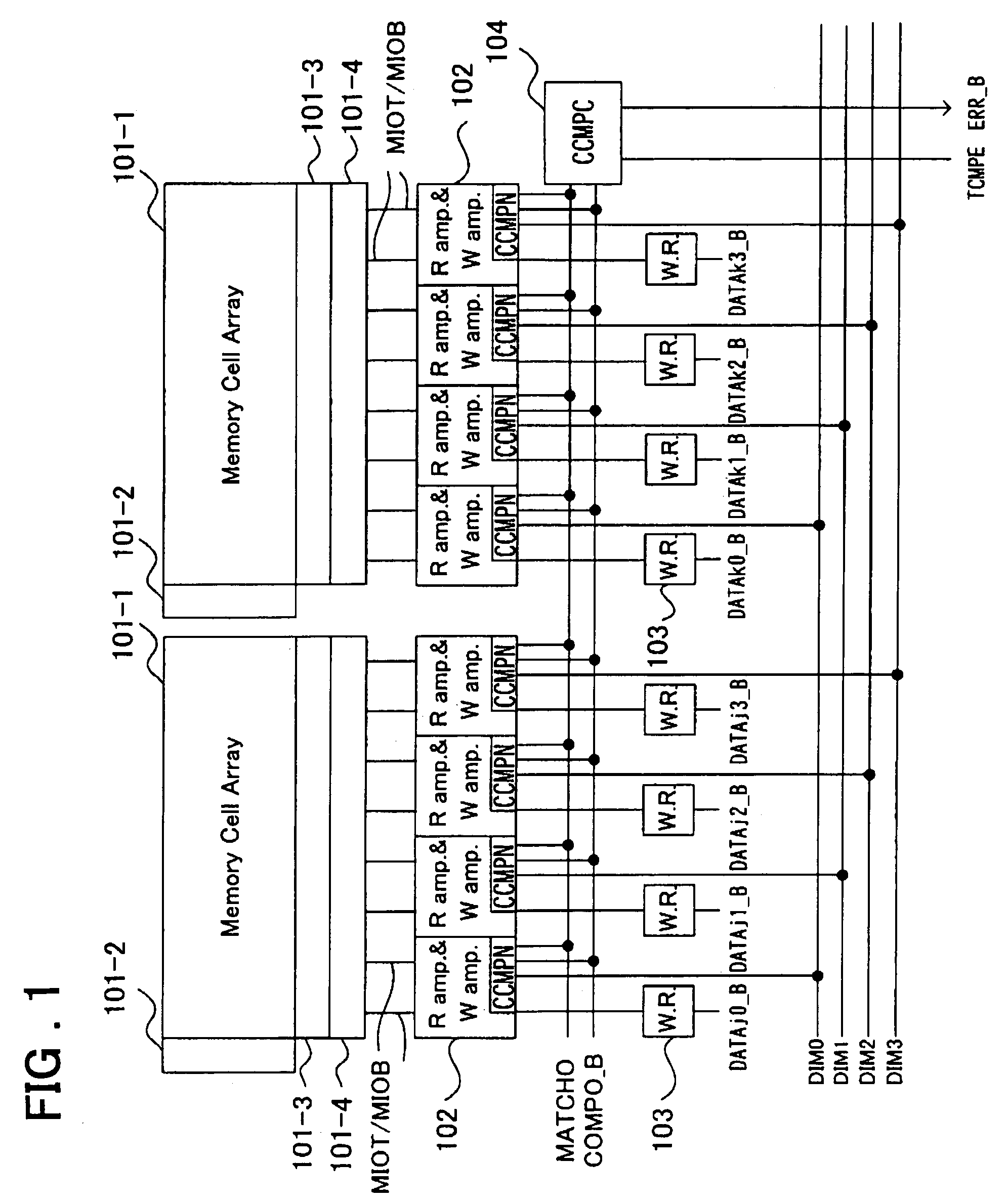
Figure 2 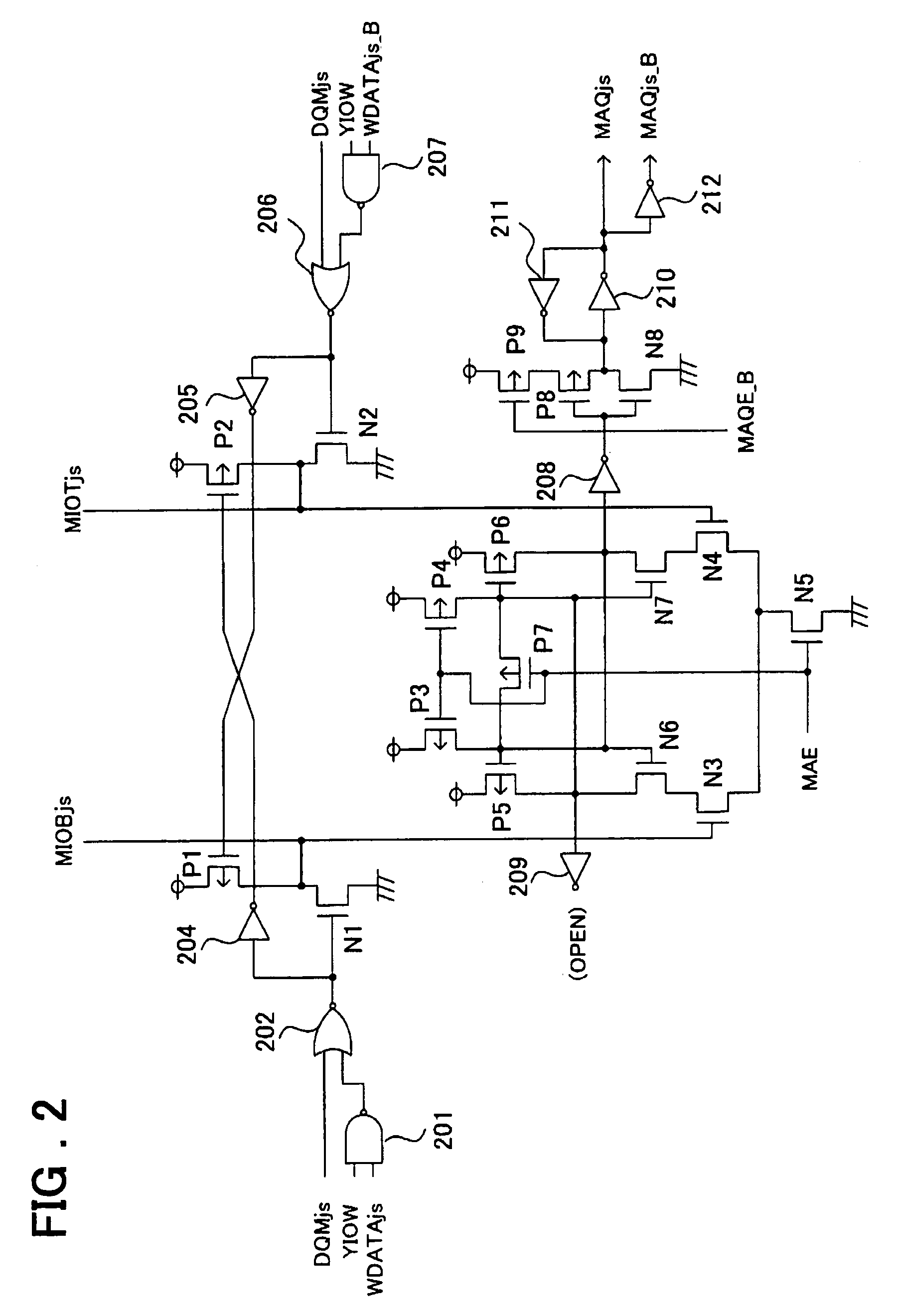
Figure 3
Abstract
Description
FIELD OF THE INVENTION
[0001] This invention relates to a semiconductor storage device and, more particularly, to a semiconductor storage device convenient for parallel testing employing a testing device.BACKGROUND OF THE INVENTION
[0002] As a parallel test, employing a testing device, a line mode test for semiconductor devices has become known (see for example the non-patent publication 1). First, the line mode test is briefly explained. FIG. 13 shows the structure of a semiconductor storage device disclosed in the non-patent publication 1. The storage device shown in FIG. 13 includes a multi-purpose register MPR (write / expectation value register) 1101 and a comparator circuit 1102 for complementary sub-IO lines SIO_T, SIO_B (bit line pair). The comparator circuit 1102 is formed by an Ex-OR circuit, and an output signal (coincidence detection signal) MATCH is wired-OR connected. The multi-purpose register MPR 1101, comprising a flip-flop formed by cross-connection of an output and an i...
Examples
embodiments
[0053]An embodiment of the present invention is now explained in further detail. FIG.1 is a schematic block diagram showing the structure of an embodiment of the present invention. The semiconductor storage device of the present embodiment has a pre-fetch function, such as an SDRAM (synchronous DRAM) or RDRAM (trademark of a product by Rambus Inc.) A write register for storage of pre-fetched data is used as a write register and as an expectation register for a parallel test, and the value of the write register is inverted and restored based on an inversion control signal from an external terminal. Referring to FIG.1, four write registers 103 and four read / write amplifiers (Ramp and Wamp) 102 are provided for a memory cell array 101-1, and each read / write amplifier (Ramp and Wamp) 102 is provided with a comparator (CCMPN) for comparing readout data and the expectation data to each other. Referring to FIG.1, the memory cell array 101-1 is provided with an X-decoder 101-2, supplied wit...