Chip resistor

A chip resistor and resistor body technology, applied in resistors, thick film resistors, resistor parts and other directions, can solve problems such as adverse effects, hinder the manufacturing yield, hinder the low resistance of chip resistors 1, etc. Good manufacturing yield and the effect of securing installation strength

Active Publication Date: 2012-08-15
KAO CORP
View PDF1 Cites 0 Cited by
  • Summary
  • Abstract
  • Description
  • Claims
  • Application Information

AI Technical Summary

Problems solved by technology

[0005] As mentioned above, although a low resistance and low TCR chip resistor can be realized by making the main component of the resistor body a copper / nickel alloy, however, in Figure 5 In the conventional chip resistor 1 shown, since the inductance of the end electrode 6 cannot be ignored, it is difficult to further reduce the resistance
That is, the chip resistor 1 mounted on the wiring pattern 31 of the circuit board 30 is energized to the upper electrode 4 or the resistor body 3 through the end electrode 6, but since the end electrode 6 extends from the lower end to the upper end of the ceramic substrate 2, A resistance value that hinders the reduction of the resistance of the chip resistor 1 is inevitably generated in the end electrode 6
[0006] In addition, this kind of chip resistor is manufactured by first dividing a large substrate for the preparation of a plurality of strips into strips, and then dividing the strip substrate into individual pieces. However, in the above-mentioned conventional chip In the case of the resistor 1, since the resistor body 3 mainly composed of a copper / nickel alloy is formed across the primary division opening groove of the large substrate, there is a problem of dividing the large substrate into long strips along the separation groove. Problems such as obstructions caused by shaped operations that adversely affect manufacturing yields

Method used


Image

  • Chip resistor
  • Chip resistor
  • Chip resistor

Examples


Embodiment Construction

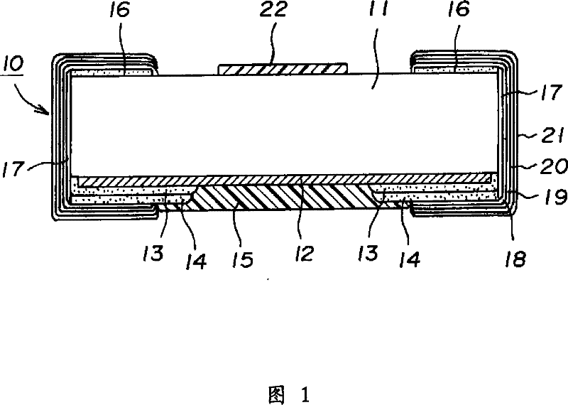
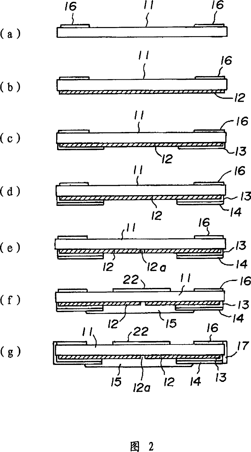
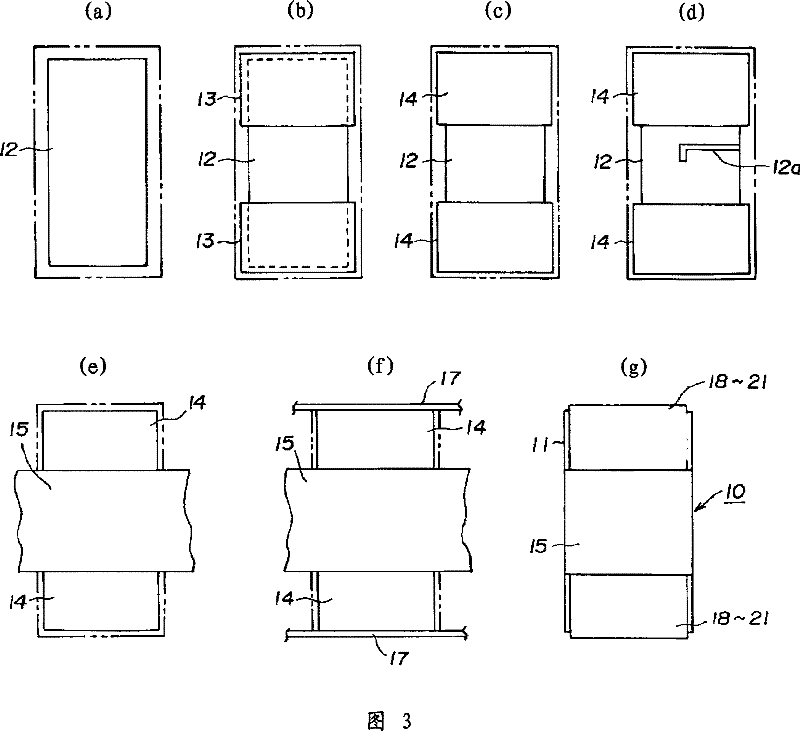
[0020] Embodiments of the invention will be described with reference to the drawings, figure 1 is a cross-sectional view schematically showing a chip resistor according to an embodiment of the present invention, figure 2 is a cross-sectional view showing the manufacturing process of the chip resistor, image 3 is a plan view showing the manufacturing process of the chip resistor, Figure 4 It is a cross-sectional view of main parts showing the state in which the chip resistor is mounted on a circuit board.

[0021] The chip resistor 10 shown in these figures is a low resistance and low TCR chip resistor mounted face down on a circuit board 30 . This chip resistor 10 is provided on the lower surface of a rectangular parallelepiped ceramic substrate 11: a resistor body 12 mainly composed of a copper / nickel alloy; The second electrode layer 13, 14; and the insulating protective layer 15 of the resistor 12 covering the area not covered by the two electrode layers 13, 14, and a...


PUM


Abstract

The invention provides a chip resistor capable of easily promoting resistance reduction and increasing a yield. The chip resistor (10) includes a box-shaped ceramic substrate (11), a resistor (12) formed of a copper / nickel alloy of a low resistance and a low TCR as a main component and arranged on the lower surface of the ceramic substrate (11), a first and a second electrode layer (13, 14) having a two-layer structure and covering the both end portions in the longitudinal direction of the resistor (12), and an insulating protection layer (15) covering the remaining region of the resistor (12). The resistor (12) is formed in a region inside the periphery of the lower surface of the ceramic substrate (11). End face electrodes (17) are provided at the opposide end faces of the ceramic substrate (11) in the length-wise direction. The second electrode layer (14) and an end face electrode (17) are covered with plating layers (18-21). The chip resistor (10) is face-down arranged with the both electrode layers mounted on a wiring pattern (31) of a circuit board (30).

Description

technical field [0001] The present invention relates to chip resistors, and more particularly to low-resistance chip resistors used for current detection and the like in circuits. Background technique [0002] A chip resistor is configured by placing a resistor made of ruthenium oxide or the like between a pair of electrodes. However, chip resistors used for current detection in circuits need to have a resistance value set to 1Ω or less in advance. In order to obtain such a low-resistance chip resistor, there has been known a technique of using a resistor mainly composed of copper (for example, refer to Patent Document 1: Japanese Unexamined Patent Publication No. 10-144501, pp. 4-5, figure 1 ). [0003] Figure 5 It is a cross-sectional view schematically showing a conventionally known low-resistance chip resistor. In the chip resistor 1 shown in this figure, a resistor body 3 mainly composed of copper / nickel alloy is provided on the upper surface of a rectangular parall...

Claims


Application Information

Patent Timeline
Patent Type & Authority Patents(China)
IPC IPC(8): H01C7/00H01C17/06
CPCH01C1/142H01C17/006H01C1/012H01C7/003
Inventor 浦野幸一赤羽泰
Owner KAO CORP
Why Eureka
Try Eureka