Supercharge Your Innovation With Domain-Expert AI Agents!

Light emitting diode crystal grain and manufacture method thereof

A technology for light-emitting diodes and a manufacturing method, which is applied to electrical components, circuits, semiconductor devices, etc., can solve the problems of low light extraction efficiency and uneven current distribution in light-emitting diode crystal grains, so as to improve light extraction efficiency and increase uniformity. Effect

Inactive Publication Date: 2015-06-03
HONG FU JIN PRECISION IND (SHENZHEN) CO LTD +1
View PDF7 Cites 0 Cited by
  • Summary
  • Abstract
  • Description
  • Claims
  • Application Information

AI Technical Summary

Problems solved by technology

In order to prevent the light emitted by the active layer from being blocked by the electrode, the area of ​​the electrode is usually set relatively small. At this time, the current density at the position below the electrode is relatively high, and the current density at the position away from the electrode is relatively small, thus The current distribution in the n-type semiconductor layer of the LED grain is uneven, and the light extraction efficiency of the LED grain is low

Method used


Image

  • Light emitting diode crystal grain and manufacture method thereof
  • Light emitting diode crystal grain and manufacture method thereof
  • Light emitting diode crystal grain and manufacture method thereof

Examples


Embodiment Construction

[0027] The present invention will be further described below with specific examples.

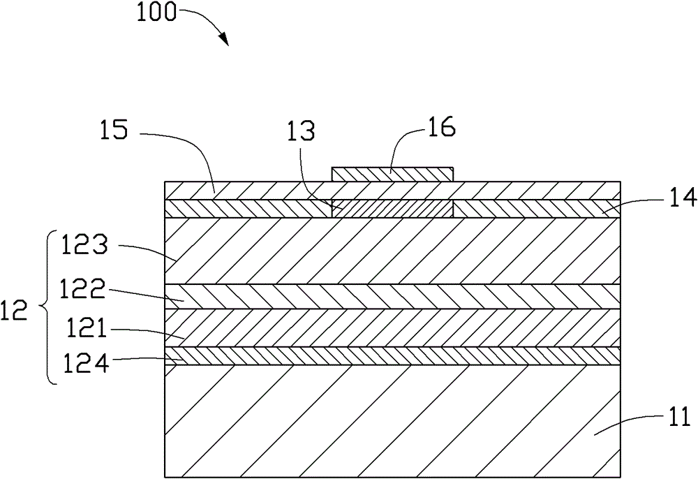
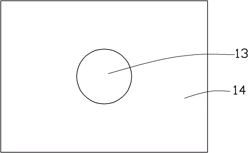
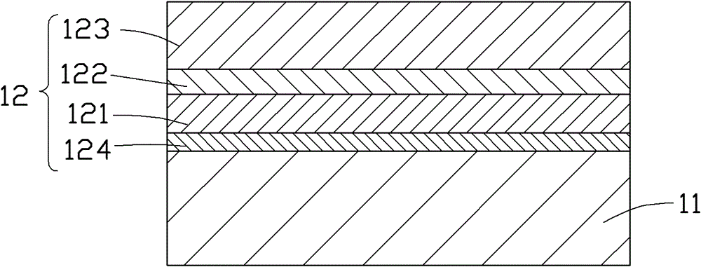
[0028] See figure 1 The light emitting diode die 100 provided by the embodiment of the present invention includes a substrate 11 and a semiconductor light emitting structure 12 disposed on the substrate 11 . A metal layer 13 and a buffer layer 14 are disposed on the surface of the semiconductor light emitting structure 12 , wherein the buffer layer 14 is disposed around the metal layer 13 . A transparent conductive layer 15 is provided on the surface of the metal layer 13 and the buffer layer 14 . An electrode layer 16 is provided on the surface of the transparent conductive layer 15 .

[0029] The substrate 11 is made of a material with high thermal conductivity, which can be a substrate made of metal materials such as copper, aluminum, nickel, silver, gold, or an alloy formed by any two or more metals, or a substrate with good thermal conductivity. Ceramic substrates such as silicon sub...


PUM


Abstract

The invention relates to a light emitting diode crystal grain comprising a substrate, a semiconductor light emitting structure, a metal layer, a buffering layer, wherein the semiconductor light emitting structure is arranged on the substrate; a transparent conductive layer is arranged on the surface of the semiconductor light emitting structure, an electrode layer is arranged on the surface of the transparent conductive layer; the buffering layer is arranged around the metal layer; the metal layer and the buffering layer are arranged between the transparent conductive layer and the semiconductor light emitting structure; schottky contact is formed between the metal layer and the semiconductor light emitting structure; and ohmic contact is formed between the buffering layer and the semiconductor light emitting structure. Since the schottky contact is formed between the metal layer and the semiconductor light emitting structure, the ohmic contact is formed between the buffering layer and the semiconductor light emitting structure, and a contact resistance of the schottky contact is bigger, electric current is diffused towards edges of the light emitting diode crystal grain, and further the uniformity of the electric current distribution is increased.

Description

technical field [0001] The invention relates to a light-emitting diode grain and a manufacturing method thereof. Background technique [0002] A light emitting diode (Light Emitting Diode, LED) is a semiconductor element that can convert electric current into light in a specific wavelength range. Light-emitting diodes can be widely used as light sources in the field of lighting because of their advantages such as high brightness, low operating voltage, low power consumption, easy matching with integrated circuits, simple driving, and long life. [0003] A light emitting diode grain generally includes a p-type semiconductor layer, an active layer, an n-type semiconductor layer, and electrodes formed on the p-type semiconductor layer and the n-type semiconductor layer. When a voltage is applied to the electrodes at both ends of the LED grain, holes and electrons will recombine in the active layer and emit photons. One of the problems faced by LED grains in the application pr...

Claims


Application Information

Patent Timeline
Patent Type & Authority Patents(China)
IPC IPC(8): H01L33/36H01L33/40
Inventor 赖志成
Owner HONG FU JIN PRECISION IND (SHENZHEN) CO LTD
Features
  • R&D
  • Intellectual Property
  • Life Sciences
  • Materials
  • Tech Scout
  • Unparalleled Data Quality
  • Higher Quality Content
  • 60% Fewer Hallucinations
Learn More