
A method to reduce the loading effect of silicon etching
A technology of etching load and effect, applied in the direction of electrical components, semiconductor/solid-state device manufacturing, circuits, etc., to achieve the effect of improving silicon etching load effect and solving manufacturing process problems
- Summary
- Abstract
- Description
- Claims
- Application Information
AI Technical Summary
Problems solved by technology
Method used
Image

Examples
Embodiment 1
[0044] Embodiment 1 of the present invention mainly comprises following specific steps:
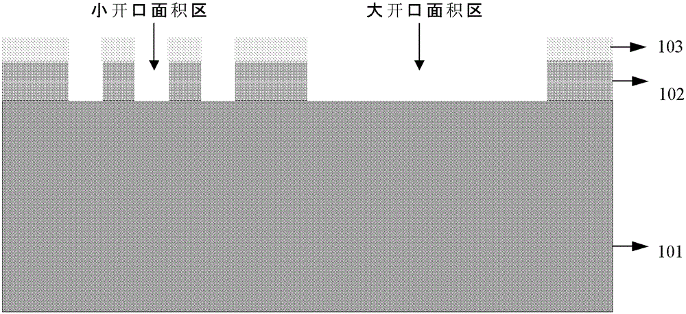
[0045] 1. If image 3 As shown, one or more dielectric films are deposited on the silicon substrate 101 as the hard mask layer 102, for example, a layer of dielectric film (such as an oxide film) can be deposited on the silicon substrate 101 as the hard mask layer 102, or An oxide film with a thickness of 125 angstroms and a SiN film with a thickness of 1500 angstroms are deposited on the silicon substrate 101 as the hard mask layer 102, because the oxide film acts as a buffer layer between the silicon substrate 101 and the SiN film, so image 3Only one layer of film (ie, the hard mask layer 102, which includes an oxide film and a SiN film) is drawn. Then apply the photoresist 103 for the first time, develop it, and make a pattern of the hard mask layer, including a large opening area area and a small opening area area. Then the hard mask layer 102 is etched, stopping on the silicon sub...
Embodiment 2
[0051] In order to achieve the purpose of removing the oxide film in the area with a large opening area and retaining the oxide film in the area with a small opening area, there is another alternative, that is, Embodiment 2. Embodiment 2 mainly comprises following specific steps:
[0052] 1. If Figure 5 As shown, one or more dielectric films are deposited on the silicon substrate 101 as the hard mask layer 102, for example, a layer of dielectric film (such as an oxide film) can be deposited on the silicon substrate 101 as the hard mask layer 102, or An oxide film with a thickness of 125 angstroms and a SiN film with a thickness of 1500 angstroms are deposited on the silicon substrate 101 as the hard mask layer 102, because the oxide film acts as a buffer layer between the silicon substrate 101 and the SiN film, so image 3 Only one layer of film (i.e. hard mask layer 102, which includes oxide film and SiN film) is drawn; then the photoresist 103 is coated for the first time,...
Embodiment 3
[0057] Embodiment 3 of the present invention mainly comprises following specific steps:
[0058] 1. If image 3 As shown, one or more dielectric films are deposited on the silicon substrate 101 as the hard mask layer 102, for example, a layer of dielectric film (such as an oxide film) can be deposited on the silicon substrate 101 as the hard mask layer 102, or An oxide film with a thickness of 125 angstroms and a SiN film with a thickness of 1500 angstroms are deposited on the silicon substrate 101 as the hard mask layer 102, because the oxide film acts as a buffer layer between the silicon substrate 101 and the SiN film, so image 3 Only one layer of film (ie, the hard mask layer 102, which includes an oxide film and a SiN film) is drawn. Then apply the photoresist 103 for the first time, develop it, and make a pattern of the hard mask layer, including a large opening area area and a small opening area area. Then the hard mask layer 102 is etched, stopping on the silicon su...
PUM
| Property | Measurement | Unit |
|---|---|---|
| thickness | aaaaa | aaaaa |
| thickness | aaaaa | aaaaa |
| thickness | aaaaa | aaaaa |
Abstract
Description
Claims
Application Information