Resistor switching circuit, storage circuit and consumable chip

A technology of switching circuits and consumable chips, applied in information storage, static memory, read-only memory, etc., can solve problems such as data transmission

Active Publication Date: 2015-09-30
APEX MICROELECTRONICS CO LTD
View PDF5 Cites 10 Cited by
  • Summary
  • Abstract
  • Description
  • Claims
  • Application Information

AI Technical Summary

Problems solved by technology

And this kind of data cannot be directly transmitted

Method used


Image

  • Resistor switching circuit, storage circuit and consumable chip
  • Resistor switching circuit, storage circuit and consumable chip
  • Resistor switching circuit, storage circuit and consumable chip

Examples


Embodiment Construction

[0036] The implementation of the present invention will be described in detail below in conjunction with the accompanying drawings and examples, so as to fully understand and implement the process of how to apply technical means to solve technical problems and achieve technical effects in the present invention. It should be noted that, as long as there is no conflict, each embodiment and each feature in each embodiment of the present invention can be combined with each other, and the formed technical solutions are all within the protection scope of the present invention.

[0037] Also, in the following description, for purposes of explanation, numerous specific details are set forth in order to provide a thorough understanding of embodiments of the invention. It will be apparent, however, to one skilled in the art that the present invention may be practiced without the specific details or in the particular manner described.

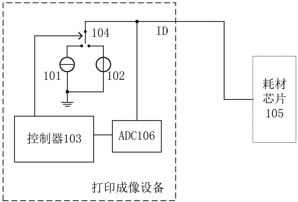
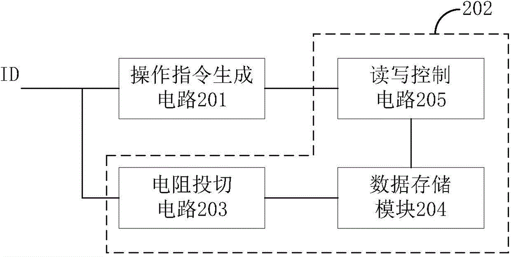
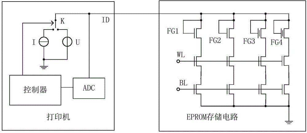
[0038] Some of the existing printing and imaging eq...


PUM


Abstract

The invention discloses a resistor switching circuit, a storage circuit and a consumable chip. The resistor switching circuit is used in the consumable chip, and comprises a plurality of resistor switching branch circuits and a decoder, wherein each resistor switching branch circuit comprises a switching switch and a resistor which are connected in series into the conducting loop of a signal wire; the decoder is connected with a data storage module in the consumable chip, and is used for outputting a switching instruction according to a signal output by the data storage module to control the switching switch of the corresponding resistor switching branch circuit to connect the corresponding resistor into the conducting loop of the signal wire or separate the resistor from the conducting loop of the signal wire, so as to change the resistance value in the conducting loop of the signal wire. The consumable chip comprising the resistor switching circuit is easy to modify, and is suitable for printing image equipment which accesses data of the consumable chip through a voltage source and current, so as to be convenient to maintain, and improve the recycling efficiency more conveniently.

Description

[0001] Cross References to Related Art [0002] This application claims the priority of Chinese patent application CN201410715520.0 filed on November 28, 2014, entitled: "A signal source identification circuit and a consumable chip including the circuit", the entire content of which is incorporated herein by reference . technical field [0003] The invention relates to the technical field of printing and imaging, in particular to a resistance switching circuit, a storage circuit and a consumable chip. Background technique [0004] The equipment used for printing and imaging has been diversified, and the widely used printing and imaging equipment mainly includes: inkjet printers, laser printers, LED printers, dot matrix printers and thermal printers. During the printing process, the printing imaging device consumes coloring materials such as ink and toner, and these coloring materials are often placed in a consumable box for convenient replenishment or replacement. [0005...

Claims


Application Information

Patent Timeline
IPC IPC(8): G11C16/10G11C16/06G11C16/26
CPCB41J2/17546H03M11/24G11C7/00G11C13/0002G11C13/0004G11C13/0023G11C13/0069G11C7/109G11C7/20
Inventor 孙万里
Owner APEX MICROELECTRONICS CO LTD
Why Eureka
Try Eureka