
Switching frequency adjusting method based on current cross feedback
A technology of cross feedback and switching frequency, which is applied in the direction of adjusting electrical variables, control/regulation systems, and converting DC power input to DC power output, etc., to achieve the effects of simple and effective control, good stability, and good power sharing effect
- Summary
- Abstract
- Description
- Claims
- Application Information
AI Technical Summary
Problems solved by technology
Method used
Image

Examples
Embodiment
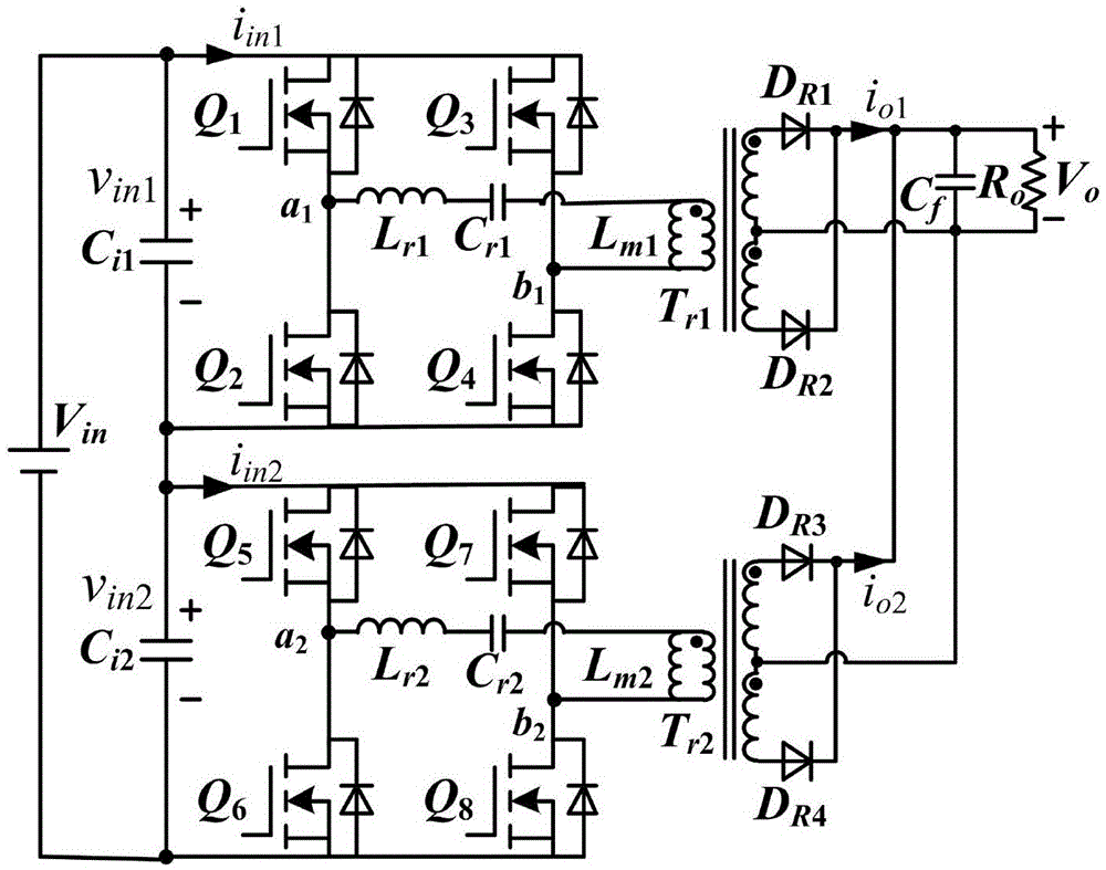
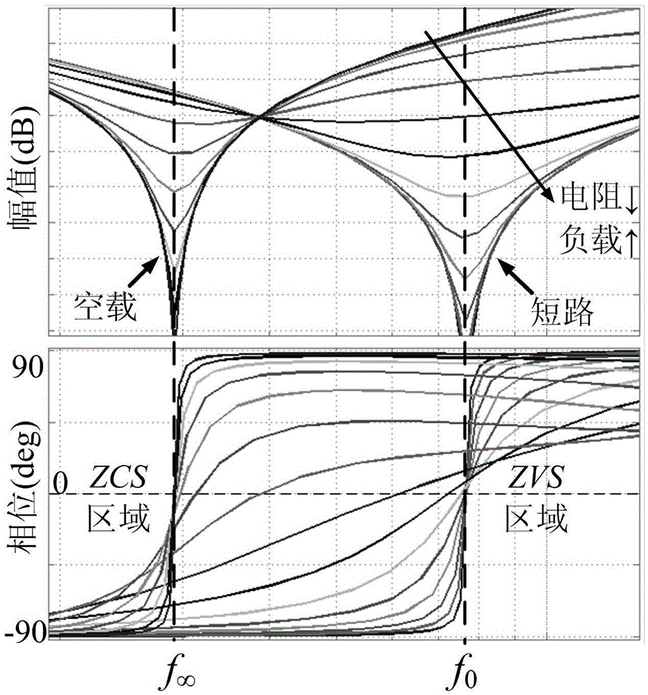
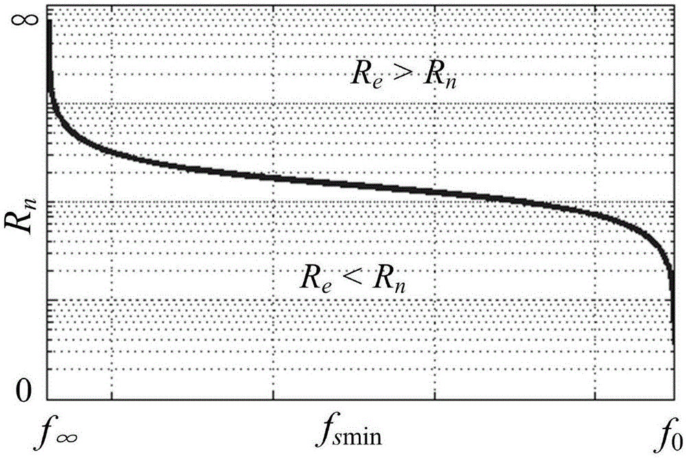
[0028] Taking a converter used in a battery charger as an example, its input voltage is 520V to 600V DC, its output voltage is 50V, and its power is 1.25kW. Using input series output parallel two modules LLC resonant DC-DC converter circuit, based on such as figure 1 The circuit shown is realized, and its component module is a full-bridge LLC circuit. In the figure v in is the total input voltage, v o is the total output voltage, Q 1 ~Q 8 It is the switching tube of the primary side of the two modules, and a 400V withstand voltage MOSFET switching tube can be used. D. R1 ~D R4 is the rectifier diode on the secondary side. C i is the input capacitance of each module, C f is the total output capacitance, R o for the total load. L r ,C r , L m are the resonant inductance, resonant capacitor and magnetizing inductance of each module respectively. T r is the transformer, N 1 ,N 2 is the transformer ratio. According to the traditional LLC design method, the resona...
PUM
 Abstract
Description
Claims
Application Information