A kind of multi-stage serial-to-parallel conversion circuit

A technology for converting circuits and circuits, applied in the direction of logic circuit connection/interface layout, logic circuit coupling/interface using field effect transistors, etc. problem, to achieve the effect of reducing logic, reducing the number of flip-flops, and increasing the maximum speed

CN105591645BActive Publication Date: 2018-11-06CAPITAL MICROELECTRONICS
3 Cites 0 Cited by

Patent Information

Authority / Receiving Office
CN · China
Patent Type
Patents(China)
Current Assignee / Owner
Publication Date
2018-11-06

Smart Images

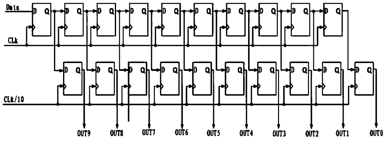
  • Figure 1
    Figure 1
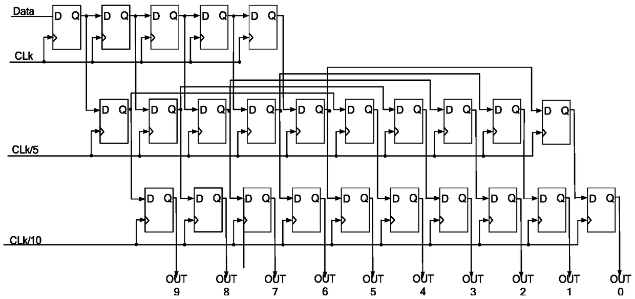
  • Figure 2
    Figure 2
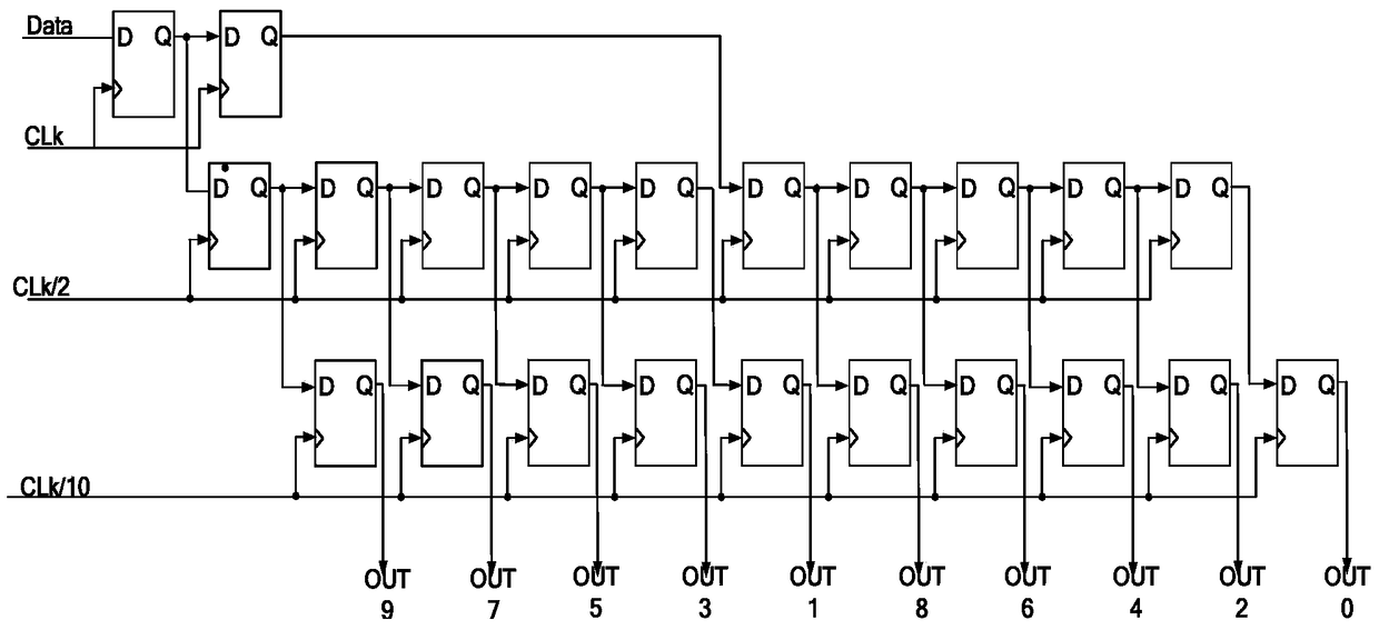
  • Figure 3
    Figure 3
Patent Text Reader

Abstract

The invention discloses a multistage serial-parallel conversion circuit, which is characterized by comprising at least three stages of D trigger groups. The first stage of D trigger groups comprises n cascaded D triggers with the same first clock signals; the second stage of D trigger groups comprises n*m cascaded D triggers with the same second clock signals; the third stage of D trigger groups comprises n*m cascaded D triggers with the same third clock signals; in the first stage of D trigger groups, the output end of the ath D trigger is connected with the input end of the ath D trigger in the second stage of D trigger groups; the output end of the ((m-1)*n+a)th D trigger in the second stage of D trigger groups is connected with the input end of the (m*n+a)th D trigger in the second stage of D trigger groups and is also connected with the input end of the ((m-1)*n+a)th D trigger in the third stage of D trigger groups; and n, m and a are all natural numbers, and a< / =n.
Need to check novelty before this filing date? Find Prior Art

Description

Technical field

[0001] The present invention relates to the field of digital communication, and in particular to a multi-stage serial-to-parallel conversion circuit applied in a serializer / paralleler interface. Background technique

[0002] The present invention relates to the field of electronic communication, serializer / deserializer (Serializer / DESerializer, SerDes). SerDes is an asynchronous data signal clock capture technology designed by a fully digital circuit, which is designed and implemented based on FPGA. A standard SerDes interface mainly includes the following modules: 8b / 10b encoder, 8b / 10b decoder, comma detector, parallel-to-serial converter, serial-to-parallel converter, clock and data recovery (CDR) , Digital Phase Locked Loop (Phase Locked Loop, PLL), etc. Among them, the parallel-serial converter and the serial-parallel converter are important modules designed by Serdes. They work the fastest in the entire circuit, which directly affects the jitter of the out...

Examples

Embodiment Construction

[0034] The technical solutions of the present invention will be further described in detail below through the accompanying drawings and embodiments.

[0035] figure 2 This is a circuit diagram of a multi-stage serial-to-parallel converter in Embodiment 1 of the present invention, and the multi-stage serial-to-parallel converter circuit can be applied to a serializer / paralleler interface.

[0036] Such as figure 2 As shown, the circuit of the multi-stage serial-parallel converter includes: at least three-stage D flip-flop groups;

[0037] The first-level D flip-flop group includes n cascaded D flip-flops (5 cascaded D flip-flops are taken as an example for illustration in this embodiment, that is, n=5), and n cascaded D flip-flops Have the same first clock signal CLK 1 , When the first clock signal CLK 1 When it arrives, all D flip-flops in the first-level D flip-flop group are triggered; the second-level D flip-flop group includes n×m cascaded D flip-flops (in this embodiment, 10 c...