Optical module

A technology of optical modules and optical fiber ribbons, which is applied in the field of optical communication and can solve problems such as difficulty in routing circuit boards

Active Publication Date: 2016-09-07
HISENSE BROADBAND MULTIMEDIA TECH
View PDF5 Cites 2 Cited by
  • Summary
  • Abstract
  • Description
  • Claims
  • Application Information

AI Technical Summary

Problems solved by technology

[0006] An embodiment of the present invention provides an optical module, which is used to solve the problem of difficul

Method used


Image

  • Optical module
  • Optical module
  • Optical module

Examples


Embodiment Construction

[0026] In order to make the technical problems, technical solutions and effects solved by the present invention clearer, the preferred embodiments of the present invention will be described below in conjunction with the accompanying drawings. It should be understood that the preferred embodiments described here are only used to illustrate and explain the present invention. Invention is not intended to limit the present invention. And in the case of no conflict, the embodiments in the present application and the features in the embodiments can be combined with each other.

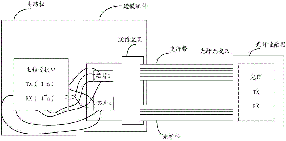
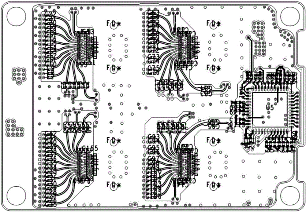
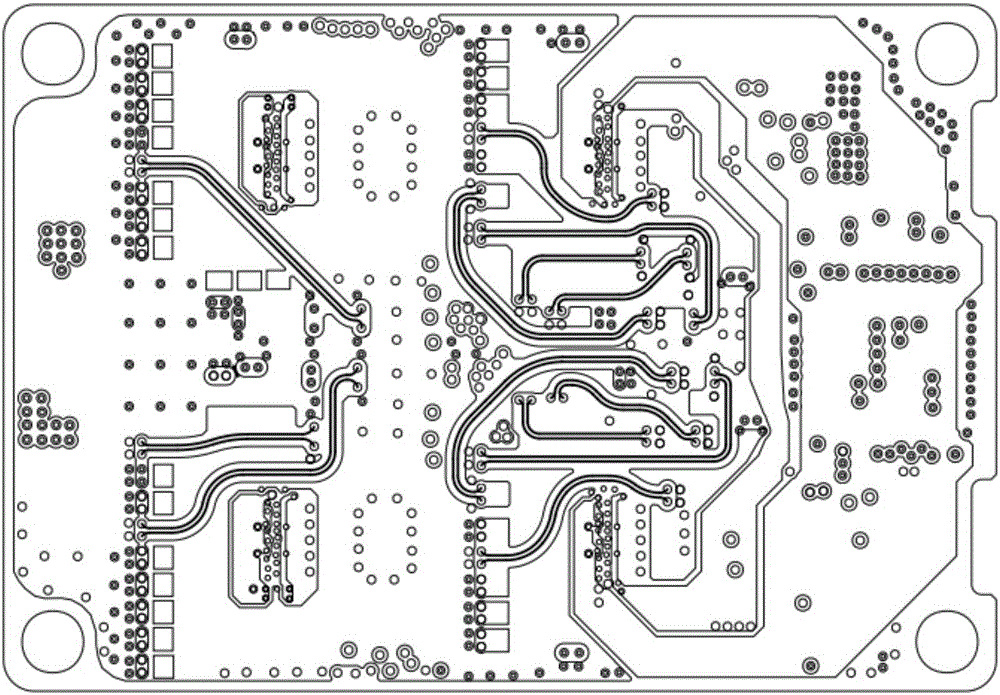
[0027] For customized optical modules or optical module designs with many channels (such as 12, 24, and 48 channels), high-speed differential signal connectors, gold fingers, etc. define the pins for transmitting and receiving electrical signals on the circuit board, The definition of fiber optic egress channels is usually derived from customer requirements or MSA regulations, and these external conditions c...


PUM


Abstract

The invention discloses an optical module and solves the problem of PCB wiring difficulty in the prior art. The optical module comprises a circuit board, a lens assembly and a fiber adapter corresponding to the lens assembly, wherein the driving chip of the lens assembly communicates with electric signal interfaces on a specific position area on the circuit board to reduce intersects of communicating channels between the electric signal interfaces on the specific position area and the driving chip. The electric signal interfaces on the specific position area are determined according to the types of the optical assemblies driven by the driving chip, and types and arrangement of each electric signal interface on the circuit board. A jumper wire device of the lens assembly communicates with the fiber adapter through an optical fiber ribbon. The sequence of the optical fiber ribbon accessing to the channels on the jumper wire device side is different from the sequence of the optical fiber ribbon accessing to the channels on the fiber adapter side. The optical module accesses the electric signal interfaces on the specific position area to the driving chip, which reduces or eliminates intersects of PCB wirings.

Description

technical field [0001] Embodiments of the present invention relate to the technical field of optical communication, and in particular, to an optical module. Background technique [0002] In the field of high-speed parallel optical modules, with the increase of optical paths, the improvement of module integration, and the continuous improvement of transmission rates, especially the multi-channel parallel optical modules with a rate of 25Gbps, the PCB board, the length of differential signal traces, and the number of vias in the module Wait for higher requirements. Cabling is becoming more and more difficult to control to an optimal level. Especially when there are many optical paths, such as high-density and high-speed parallel optical modules with 12 / 24 / 48 channels, there are usually multiple ICs that output enough high-speed differential signal channels in parallel, and the routing of high-speed differential signals on the PCB will be very complicated. It will be difficul...

Claims


Application Information

Patent Timeline
IPC IPC(8): G02B6/42
CPCG02B6/4249G02B6/4279
Inventor 徐海强
Owner HISENSE BROADBAND MULTIMEDIA TECH
Why Eureka
Try Eureka