A New Type of Transit Box for Silicon Wafers

A transfer box and silicon wafer technology, which is applied in the types of packaging items, bottle/can parts, container decorations, etc., can solve the problems of inconvenient operation, reduce production efficiency, etc. The effect of improving production and processing efficiency

Active Publication Date: 2018-02-13
江苏美科太阳能科技股份有限公司
View PDF7 Cites 0 Cited by
  • Summary
  • Abstract
  • Description
  • Claims
  • Application Information

AI Technical Summary

Problems solved by technology

[0002] After sorting polysilicon wafers in the prior art, they are divided into two categories: A-grade products and defective products. A-grade products need to be stored in foam boxes. The two categories are not distinguished by different colors, and the previous rod and the latter rod are placed in the same area without area division, which makes subsequent operations inconvenient and reduces production efficiency

Method used


Image

  • A New Type of Transit Box for Silicon Wafers
  • A New Type of Transit Box for Silicon Wafers
  • A New Type of Transit Box for Silicon Wafers

Examples


Embodiment Construction

[0020] The specific embodiments of the present invention will be further described below in conjunction with the accompanying drawings.

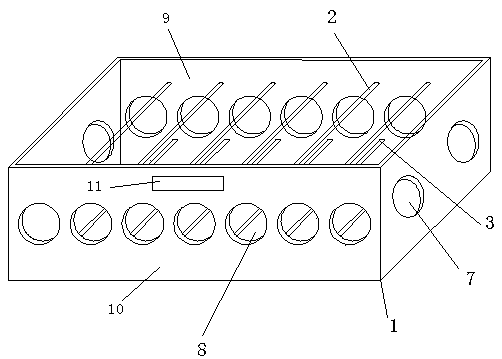
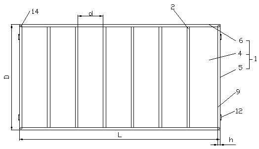
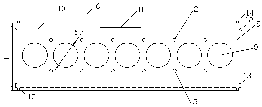
[0021] A new type of transfer box for silicon wafers, comprising a box body 1 made of PTFE, a number of first support sticks 2 and second support sticks 3, wherein the box body 1 is in the shape of a cube and includes a bottom plate 4, The first side plate 5 and the second side plate 6, the length L of the box body 1 is 360mm, the width D is 190mm, and the height H is 110mm. There are two first side plates 5, and they are respectively as wide as the bottom plate 4. The sides are vertically connected, and the first side plate 5 is provided with a plurality of first round holes 7;

[0022] Described second side plate 6 has two, and is vertically connected with base plate 4 long sides respectively, and described second side plate 6 is vertically connected with first side plate 5, and described second side plate 6 is provided with a plurality of...


PUM


Abstract

The invention relates to a novel silicon slice transfer box. The novel silicon slice transfer box comprises a box body, a plurality of first supporting sticks and a plurality of second supporting sticks. The box body comprises a base plate, first side plates and second side plates. A plurality of first circular holes are formed in the first side plates and a plurality of second circular holes are formed in the second side plates. The second circular holes and the first circular holes are uniformly distributed on the same plane at intervals. Sponge mats are arranged on the surfaces of the box body, the first supporting sticks and the second supporting sticks. The novel silicon slice transfer box is capable of subpackaging cutting silicon slices of each polycrystalline silicon bar according to different colors, convenient to transfer, easy for inspection of a quality inspector and capable of improving production efficiency.

Description

technical field [0001] The invention relates to a novel silicon wafer transfer box, which belongs to the technical field of polycrystalline silicon wafer production and processing. Background technique [0002] After sorting polysilicon wafers in the prior art, they are divided into two categories: A-grade products and defective products. The two categories are not distinguished by different colors, and the previous rod and the rear rod are placed in the same area without area division, which makes subsequent operations inconvenient and reduces production efficiency. Contents of the invention [0003] The object of the present invention is to provide a new type of transfer box for silicon wafers, which can pack cut silicon wafers of crystal ingots according to different colors, which is convenient for transfer, so as to facilitate inspection by quality inspectors and improve production efficiency. [0004] The present invention is achieved through the following technical ...

Claims


Application Information

Patent Timeline
Patent Type & Authority Patents(China)
IPC IPC(8): B65D85/30B65D25/02B65D77/28
CPCB65D25/02B65D77/28B65D85/30B65D2203/02B65D2203/12
Inventor 朱孝吉王禄宝陈董良
Owner 江苏美科太阳能科技股份有限公司
Why Eureka
Try Eureka