Graphene and transparent conductive film two-way absorbing transparent electromagnetic shielding device

A technology of transparent conductive film and graphene film, which is applied in the fields of magnetic field/electric field shielding, electrical components, chemical instruments and methods, etc., can solve the problem that it is difficult to balance high light transmittance and strong microwave shielding efficiency, transparency and conductive shielding ability. Restriction, secondary pollution and other issues, to achieve the effect of strong electromagnetic shielding, good electromagnetic shielding, low reflection and strong electromagnetic shielding

CN106413364BActive Publication Date: 2021-03-26HARBIN INST OF TECH
9 Cites 0 Cited by

Patent Information

Authority / Receiving Office
CN · China
Patent Type
Patents(China)
Current Assignee / Owner
Publication Date
2021-03-26

Smart Images

  • Figure 1
    Figure 1
  • Figure 2
    Figure 2
  • Figure 3
    Figure 3
Patent Text Reader

Abstract

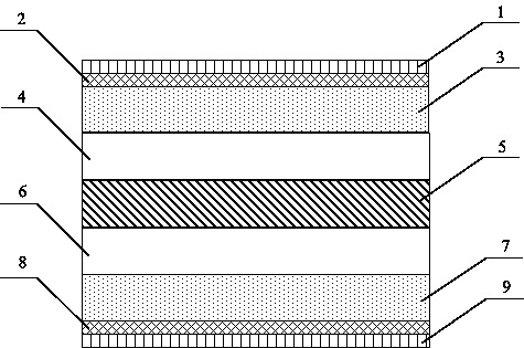
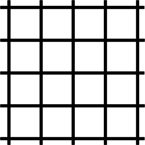
A bidirectional wave absorption transparent electromagnetic shielding device based on graphene / transparent conductive films belongs to the optical transparent member electromagnetic shielding technology field, and is formed by assembling a transparent absorption layer A, a transparent medium A, a transparent reflection layer, a transparent medium B and a transparent absorption layer B which are orderly laminated and parallelly configured. The transparent absorption layers A and B are both formed by 1-6 layers of graphene films separated by transparent mediums, and the transparent reflection layer is composed of transparent conductive films comprising transparent metal compound films, silver nanowire films or metal meshes. The electromagnetic shielding device can absorb the radio frequency radiation at the two sides of the devices simultaneously, repeatedly and strongly, thereby realizing the bidirectional strong shielding and low reflection characteristics. The electromagnetic shielding device of the present invention solves the problem that a conventional transparent electromagnetic shielding method can not consider the bidirectional low-electromagnetic reflection, the strong electromagnetic shielding and the high light transmission simultaneously, and has the characteristics of high light transmission performance, strong electromagnetic shielding and bidirectional low electromagnetic reflection.
Need to check novelty before this filing date? Find Prior Art

Description

technical field

[0001] The invention belongs to the field of electromagnetic shielding of optical transparent parts, in particular to a bidirectional wave-absorbing transparent electromagnetic shielding device based on graphene / transparent conductive film. Background technique

[0002] With the development of radio, television, wireless communication technology and microwave technology, a large number of radio frequency devices are equipped in various places of human activities, and the spectrum range continues to widen, and the intensity doubles, which not only interferes with electronic equipment, but also affects human health. threaten. This invisible and intangible "electromagnetic pollution" directly acts on machines or human bodies, and is a serious "invisible killer". It has become the fifth largest pollution after air pollution, water pollution, solid waste pollution and noise pollution. Electromagnetic shielding (including absorption and reflection) is the main mea...

Examples

Embodiment

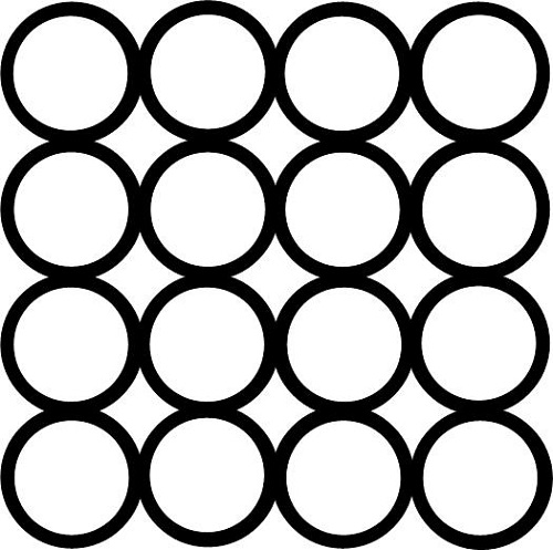
[0036] The electromagnetic shielding device is composed of a transparent absorption layer A3, a transparent medium A4, a transparent reflection layer 5, a transparent medium B6, and a transparent absorption layer B7 that are stacked and arranged in parallel in sequence; the transparent absorption layer A3 is composed of a single layer arranged in parallel The graphene film A10, the transparent medium C11 and the single-layer graphene film B12 are composed, the transparent reflective layer is composed of the micro-ring metal grid 14, and the transparent absorbing layer B7 is composed of a single-layer graphene film C13.

[0037] The technical effect of the present invention is: when the electromagnetic shielding efficiency of metal mesh grid is 19.0dB, the electromagnetic shielding efficiency of the present invention is 23.7dB, if radio frequency radiation comes from the transparent absorbing layer A3 outside of electromagnetic shielding device, absorption loss accounts for total...