Shift register and driving method, grid driving circuit and display device thereof

A technology of shift register and reset signal, applied in the field of gate drive circuit, display device, and shift register, can solve the problems of increased process difficulty, increased production cost, complicated connection structure, etc.

Inactive Publication Date: 2017-09-01
BOE TECH GRP CO LTD +1
View PDF10 Cites 20 Cited by
  • Summary
  • Abstract
  • Description
  • Claims
  • Application Information

AI Technical Summary

Problems solved by technology

At present, although the output of the scanning signal can be realized by inputting more control signals with different functions, this leads to a large number of switching transistors constituting shift registers of various levels in the gate drive circuit, and causes the gap between the switching transistors to be high. The specific structure of the inter-connection is also relatively complicated, resulting in a complex structure of the shift register, resulting in increased process difficulty and increased production costs.

Method used


Image

  • Shift register and driving method, grid driving circuit and display device thereof
  • Shift register and driving method, grid driving circuit and display device thereof
  • Shift register and driving method, grid driving circuit and display device thereof

Examples


Embodiment 1

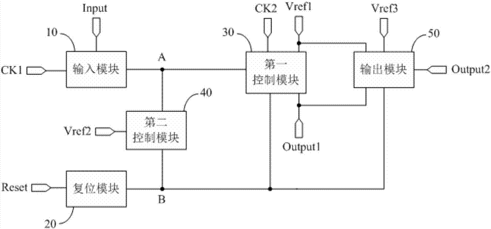
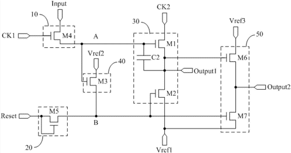
[0093] by Figure 4a The structure of the shift register shown is taken as an example to describe its working process, and the corresponding input and output timing diagrams are shown in Figure 5a As shown, specifically, the main selection such as Figure 5a There are three stages T1, T2 and T3 in the shown input and output timing diagram, and there is an inversion stage T0 in the blanking time, and the duration of the inversion stage T0 is the preset duration. Wherein, the potential of the first reference signal terminal Vref1 and the potential of the second reference signal terminal Vref2 are both low potential, and the potential of the third reference signal terminal Vref3 is high potential; The preset duration in the time Blank time is low potential, and the rest of the time is high potential.

[0094] In the T1 stage, Input=1, Reset=0, CS=1, CK1=1, CK2=0.

[0095] Since CK1=1, the fourth switching transistor M4 is turned on and provides the high potential signal of th...

Embodiment 2

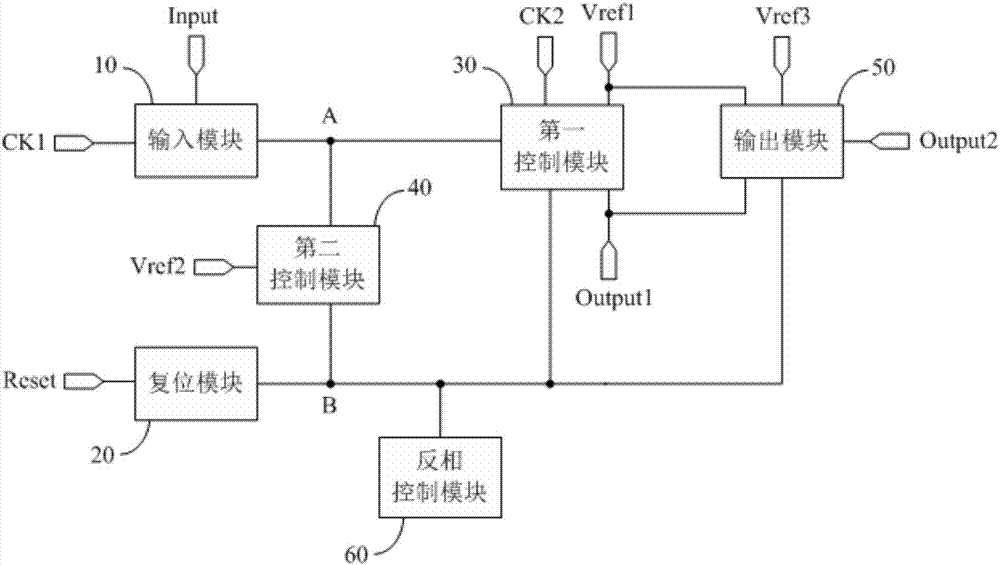
[0110] by Figure 4b The structure of the shift register shown is taken as an example to describe its working process, and the corresponding input and output timing diagrams are shown in Figure 5b As shown, specifically, the main selection such as Figure 5b There are three stages T1, T2 and T3 in the shown input and output timing diagram, and there is an inversion stage T0 in the blanking time, and the duration of the inversion stage T0 is the preset duration. Wherein, the potential of the first reference signal terminal Vref1 and the potential of the second reference signal terminal Vref2 are both high potential, and the potential of the third reference signal terminal Vref3 is low potential; The preset time in the time Blank time is high potential, and the rest of the time is low potential.

[0111] In the T1 stage, Input=0, Reset=1, CS=0, CK1=0, CK2=1.

[0112] Since CK1=0, the fourth switching transistor M4 is turned on and provides the low potential signal of the inp...


PUM


Abstract

The invention discloses a shift register and driving method, grid driving circuit and display device thereof provided by an embodiment of the invention. The shift register comprises an input module, a reset module, the first control module, the second control module and an output module; through the coordination of the above modules, the scanning signals used for inputting in the corresponding grid lines can be output through the scanning signal output end by using a simple structure, the cascade signals are output from the output end of the cascaded signal, and the cascade signals are used as the signals of the signal input ends of other cascaded shift registers, so that the cascade signal output end for outputting cascade signals is different from the scanning signal output end for outputting scanning signals, so the signal interference of the scanning signals input in the grid lines to the input signal end of the next shift register can be avoided, so that the stability of the shift register can be improved, and then the overall stability of the circuit formed by cascading the plurality of the shift registers can be improved.

Description

technical field [0001] The invention relates to the field of display technology, in particular to a shift register, a driving method thereof, a gate driving circuit and a display device. Background technique [0002] With the rapid development of display technology, the display panel is more and more developed towards the direction of high integration and low cost. Among them, the gate driver on array (Gate Driver on Array, GOA) technology integrates the thin film transistor (Thin Film Transistor, TFT) gate switching circuit on the array substrate of the display panel to form a scan drive for the display panel, so that the gate driver can be omitted. The wiring space of the Bonding area of ​​the integrated circuit (Integrated Circuit, IC) and the fan-out (Fan-out) area can not only reduce the product cost in terms of material cost and manufacturing process, but also enable the display panel to achieve Beautiful design with symmetry on both sides and narrow frame; moreover, ...

Claims


Application Information

Patent Timeline
Patent Type & Authority Applications(China)
IPC IPC(8): G09G3/20G11C19/28
Inventor 王迎李红敏薛伟孙丽
Owner BOE TECH GRP CO LTD
Why Eureka
Try Eureka