Flexible substrate of OLED display panel and preparation method thereof

A flexible substrate and display panel technology, applied in the direction of final product manufacturing, climate sustainability, sustainable manufacturing/processing, etc., can solve the problems of PI layer damage, PI layer protection effect is not obvious, affecting the quality of OLED display panels, etc. Achieve the effect of reducing transmittance, improving product yield, and increasing absorption

Active Publication Date: 2017-12-22
WUHAN CHINA STAR OPTOELECTRONICS SEMICON DISPLAY TECH CO LTD
View PDF4 Cites 16 Cited by
  • Summary
  • Abstract
  • Description
  • Claims
  • Application Information

AI Technical Summary

Problems solved by technology

[0007] The invention provides a method for preparing a flexible substrate of an OLED display panel. The buffer layer of the flexible substrate can weaken the damage of the laser to the PI layer, so as to solve the protect

Method used


Image

  • Flexible substrate of OLED display panel and preparation method thereof
  • Flexible substrate of OLED display panel and preparation method thereof

Examples


Embodiment Construction

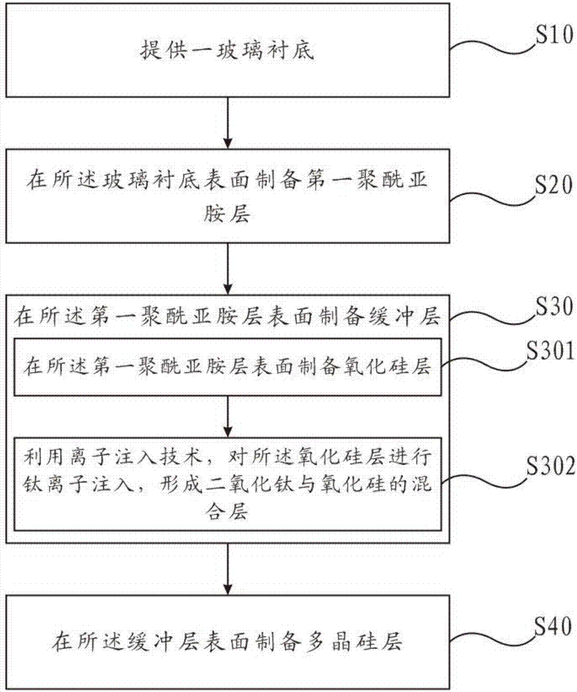
[0036] The following descriptions of the various embodiments refer to the accompanying drawings to illustrate specific embodiments in which the invention may be practiced. The directional terms mentioned in the present invention, such as [top], [bottom], [front], [back], [left], [right], [inside], [outside], [side], etc., are only for reference The orientation of the attached schema. Therefore, the directional terms used are used to illustrate and understand the present invention, but not to limit the present invention. In the figures, structurally similar elements are denoted by the same reference numerals.

[0037] The present invention is aimed at the buffer layer of the flexible substrate of the existing OLED display panel, which has no obvious protective effect on the PI layer and is likely to cause damage to the PI layer, thereby affecting the quality of the OLED display panel. This embodiment can solve this defect.

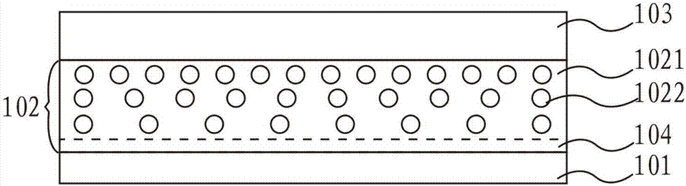
[0038] Such as figure 1 As shown, the flexible sub...


PUM


Abstract

The invention provides the preparation method of the flexible substrate of an OLED display panel. The method comprises the steps that S10 a glass substrate is provided; S20 a first polyimide layer is prepared on the surface of the glass substrate; and S30 a buffer layer is prepared on the surface of the first polyimide layer. The step S30 comprises the steps that S301 a silicon oxide layer is prepared on the surface of the first polyimide layer; and S302 an ion implantation technology is used to carry out titanium ion implantation on the silicon oxide layer to form the mixed layer of titanium oxide and silicon oxide. The preparation method has the advantages that the buffer layer of the flexible substrate of the OLED display provided by the invention can absorb more ultraviolet laser; the transmittance of ultraviolet laser is reduced; the damage of laser annealing to a PI layer is reduced; and the product yield is improved.

Description

technical field [0001] The invention relates to the technical field of liquid crystal display, in particular to a GOA circuit and a liquid crystal display panel with the GOA circuit. Background technique [0002] OLED (Organic Light-Emitting Diode, organic light-emitting diode) display, also known as organic electroluminescent display, is a new flat panel display device, due to its simple manufacturing process, low cost, low power consumption, high luminous brightness, Wide range of working temperature, light and thin volume, fast response speed, easy to realize color display and large-screen display, easy to realize matching with integrated circuit driver, easy to realize flexible display, etc., so it has broad application prospects; today, flexible OLED Panels have become an important research direction for organic light-emitting devices, and flexible substrates are chosen to replace traditional glass substrates to achieve the bendability of panels. [0003] Flexible OLED...

Claims


Application Information

Patent Timeline
IPC IPC(8): H01L51/56H01L51/00H01L51/52
CPCH10K77/111H10K50/844H10K71/00G02F2201/07H10K71/80H10K2102/311
Inventor 秦学思
Owner WUHAN CHINA STAR OPTOELECTRONICS SEMICON DISPLAY TECH CO LTD
Why Eureka
Try Eureka