Flexible display panel, flexible display device and preparation method of flexible display panel

A flexible display and flexible substrate technology, applied in chemical instruments and methods, climate sustainability, and other household appliances, can solve problems such as low bending resistance, abnormal screen display, and easy wear and tear of electronic components, so as to reduce Effects of stress change, reduction of wear, and probability of abnormal screen display

Active Publication Date: 2018-04-24
HEFEI XINSHENG OPTOELECTRONICS TECH CO LTD +1
View PDF7 Cites 3 Cited by
  • Summary
  • Abstract
  • Description
  • Claims
  • Application Information

AI Technical Summary

Problems solved by technology

[0006] In view of this, the present invention provides a flexible display panel, a flexible display device and a preparation method thereof. The main technical problem to be solved is that the electronic components with low bending resistance of the flexible display panel are prone to wear and tear, resulting in abnormal screen display.

Method used


Image

  • Flexible display panel, flexible display device and preparation method of flexible display panel
  • Flexible display panel, flexible display device and preparation method of flexible display panel
  • Flexible display panel, flexible display device and preparation method of flexible display panel

Examples


preparation example Construction

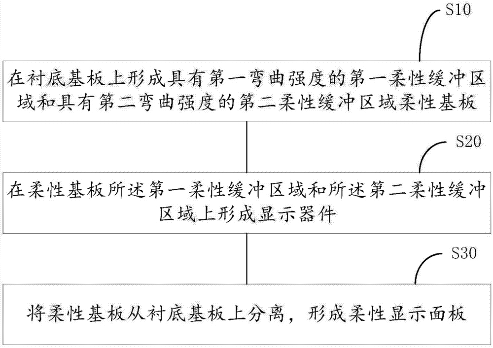
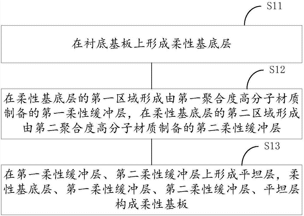
[0054] In the method for preparing a flexible display panel provided in this embodiment, two flexible buffer regions with different bending strengths are formed on the base substrate. In the display device, electronic components with low bending resistance are formed at the bending strength In the lower flexible buffer zone, the stress on the area with weaker bending strength will be dispersed to the area with stronger bending strength, which is beneficial to reduce the stress change in the area with poor stress during bending deformation and reduce wear.

[0055] Figure 1 to Figure 2 For an example of the preparation method of the flexible display panel provided by the present invention, please refer to Figure 1 to Figure 2 , a method for preparing a flexible display panel proposed by an embodiment of the present invention, including:

[0056] S10, forming a first flexible buffer region with a first bending strength and a second flexible buffer region flexible substrate wi...


PUM


Abstract

The invention relates to a flexible display panel, a flexible display device and a preparation method of the flexible display panel and belongs to the flexible display technical field. The invention mainly aims to solve the proneness of the low-bending-resistance electronic components of a flexible display panel to being worn. The preparation method of the flexible display panel includes the following steps that: a flexible substrate provided with a first flexible buffer region having first bending strength and a second flexible buffer region having second bending strength is formed on a substrate, wherein the first bending strength is greater than the second bending strength; and a display device is formed on the flexible substrate. Electronic component with low-bending-resistance electronic components as well as a punched region and a channel region which have poor flexible stress in the display device are formed in the second flexible buffer region; and stress applied to the secondflexible buffer region with weak bending strength is dispersed to the first flexible buffer region with strong bending strength, and therefore, the reduction of the change of stress borne by display components in the poor stress region, namely, the second flexible buffer region, can be benefitted, and wear can be reduced.

Description

technical field [0001] The present invention relates to the field of flexible display technology, in particular to a flexible display panel, a flexible display device and a preparation method thereof. Background technique [0002] Organic Light Emitting Display (OLED) has excellent performances such as low power consumption, high saturation, wide viewing angle, thin thickness, and flexibility, and has gradually become the mainstream in the display field. [0003] The preparation process of traditional flexible display panels is as follows: a uniform flexible substrate is bonded and formed on a rigid substrate, and then thin film transistors and display electronic components are formed on a uniform flexible substrate, and finally the flexible substrate is separated from the rigid substrate. , a flexible display panel can be prepared. [0004] The inventor finds that there are at least the following problems in the prior art: [0005] During the bending of the flexible displ...

Claims


Application Information

Patent Timeline
Patent Type & Authority Applications(China)
IPC IPC(8): H01L27/32H01L51/00H01L21/77
CPCH10K59/12H10K77/111H10K59/1201Y02E10/549Y02P70/50H10K71/80H10K2101/00H10K2102/311H10K71/00B32B3/266B32B2457/206B32B27/281B32B27/32B32B27/08
Inventor 贾文斌王欣欣叶志杰彭锐窦义坤胡月宋丽芳孙力
Owner HEFEI XINSHENG OPTOELECTRONICS TECH CO LTD
Why Eureka
Try Eureka