Full-automatic exposure technology

A fully automatic and high-tech technology, applied in the field of PCB exposure, can solve the problems of manual operation and low production efficiency of exposure machines, and achieve the effects of improving exposure efficiency, improving efficiency, and shortening processing time

Inactive Publication Date: 2018-07-24
CHENGDU KAIJING INTELLIGENT EQUIP CO LTD
View PDF4 Cites 5 Cited by
  • Summary
  • Abstract
  • Description
  • Claims
  • Application Information

AI Technical Summary

Problems solved by technology

[0005] The purpose of the present invention is to provide a fully automatic exposure process in order to solve the problem that the exposure machine in the prior art requires manual operation, resulting in low production efficiency

Method used


Image

  • Full-automatic exposure technology
  • Full-automatic exposure technology

Examples


Embodiment 1

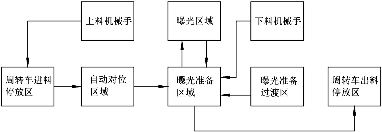
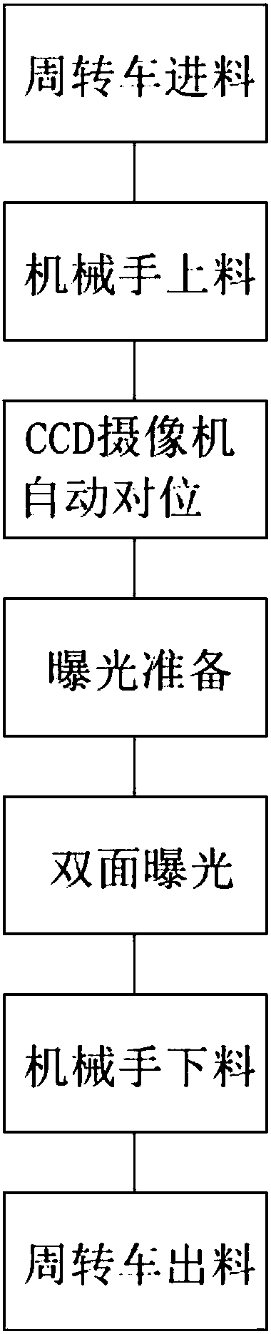
[0036] Such as figure 1 , figure 2 Shown, a kind of automatic exposure process is characterized in that, comprises the following steps:

[0037] A. Feed material: The PCB board turnover vehicle transports the PCB boards that need to be exposed from the upper process of the exposure machine, and parks them in the parking area 1 of the PCB board turnover vehicle.

[0038] B. Loading: The loading manipulator grabs the PCB boards on the PCB board turnover car to the automatic alignment area in sequence for alignment.

[0039] C. Automatic alignment: Through the CCD camera and visual alignment system, the automatic alignment of the upper film and the lower film, and the automatic alignment of the film and the PCB board are completed.

[0040] D. Exposure preparation: Grab the aligned PCB board into the exposure preparation area by the handling manipulator, complete the overlapping of the PCB board and the upper and lower negatives, and check it through the CCD camera system.

...

Embodiment 2

[0046] This embodiment focuses on the differences from the above embodiments, and the similarities will not be repeated. In this embodiment, an exposure room is provided in the exposure area of ​​the step E, and an upper light source and a lower light source are provided in the exposure room. , for double-sided simultaneous exposure of PCB boards.

Embodiment 3

[0048] This embodiment focuses on the differences from the above-mentioned embodiments, and the similarities will not be repeated. In this embodiment, the PCB board turnover vehicle can be hauled by an AGV trolley, and the AGV trolley is an electric power supply that can be automatically charged. The driving trolley can automatically run along the planned route, and the production points of each process can automatically call the AGV trolley through the access of the calling system.


PUM


Abstract

The invention discloses a full-automatic exposure technology and belongs to the technical field of PCB exposure. The full-automatic exposure technology comprises the following steps: A, feeding a material: a PCB transfer vehicle conveys PCBs to be exposed; B, loading the material: a material loading manipulator grabs the PCBs on the PCB transfer vehicle to an automatic aligning area to be aligned;C, automatic alignment: a CCD camera and a visual aligning system can finish automatic alignment between an upper negative film and a lower negative film, and the negative films and the PCBs are automatically aligned; D, exposure preparation: a carrying manipulator can grab the aligned PCBs to an exposure preparation area, and overlapping between the PCBs and the upper and lower negative films isfinished and is checked by a CCD camera system; E exposure: the aligned and checked PCBs are sent into the exposure area to be exposed by a lead screw guide rail platform of the exposure preparationarea, and after exposure is finished, the PCBs are automatically returned to the exposure preparation area; F, discharging the material: a discharging manipulator grabs the exposed PCBs to the PCB transfer vehicle. The full-automatic exposure technology disclosed by the invention can achieve unmanned automatic processing in the whole process.

Description

technical field [0001] The invention belongs to the technical field of PCB exposure, and in particular relates to an exposure process with fully automatic unmanned operation. Background technique [0002] PCB (Printed Circuit Board), the Chinese name is printed circuit board, also known as printed circuit board, is an important electronic component, a support for electronic components, and a carrier for electrical connections of electronic components. Because it is made using electronic printing, it is called a "printed" circuit board. [0003] In the PCB board manufacturing process, one of the most critical processes is to transfer the negative film image to the substrate: first coat a layer of photosensitive material on the substrate, and then irradiate the photosensitive material coated on the substrate to dissolve it The properties change, but the resin in the unphotosensitive part does not undergo polymerization reaction, and it will dissolve under the action of the de...

Claims


Application Information

Patent Timeline
Patent Type & Authority Applications(China)
IPC IPC(8): G03F7/20G03F9/00
Inventor 杨刚胡大宏郑亮宋凯冉林何晓蓉
Owner CHENGDU KAIJING INTELLIGENT EQUIP CO LTD
Why Eureka
Try Eureka