Organic light-emitting diode (OLED) display device

A technology of light-emitting diodes and display devices, which is applied in the direction of diodes, organic semiconductor devices, electrical components, etc., and can solve problems such as the dilemma of light extraction efficiency, the loss of brightness of organic light-emitting diode panels, and the increase in overall device thickness and weight

Active Publication Date: 2018-10-09
TRENDON TOUCH TECHNOLOGY CORPORATION
View PDF8 Cites 5 Cited by
  • Summary
  • Abstract
  • Description
  • Claims
  • Application Information

AI Technical Summary

Problems solved by technology

Although the anti-reflection optical film group with this structure solves the problem of reflection of external light, it leads to a loss of 60% of the brightness of the OLED panel, because the transmittance of a polarizer is only about 40-50%.
Therefore, the known

Method used


Image

  • Organic light-emitting diode (OLED) display device
  • Organic light-emitting diode (OLED) display device
  • Organic light-emitting diode (OLED) display device

Examples


Embodiment Construction

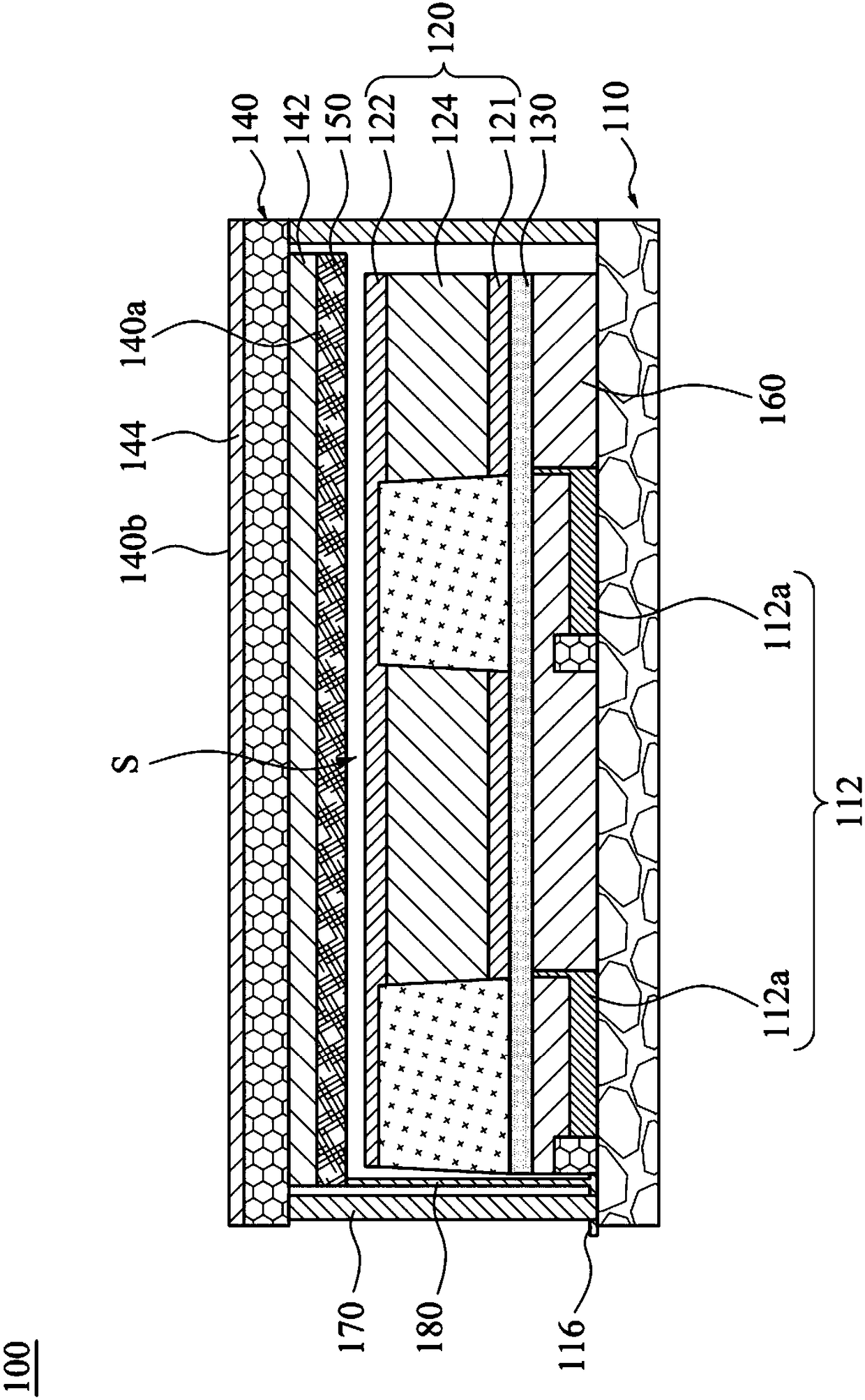
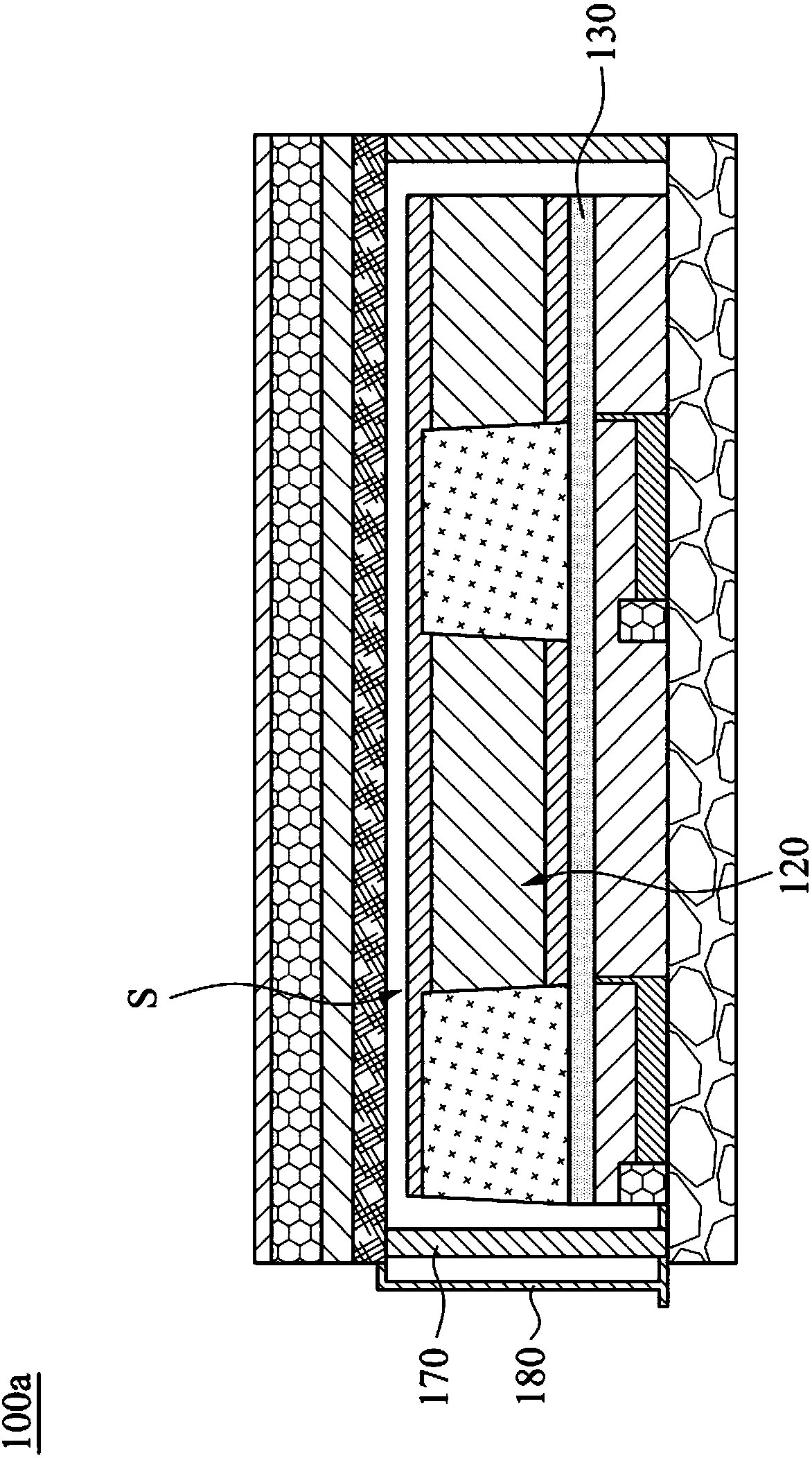
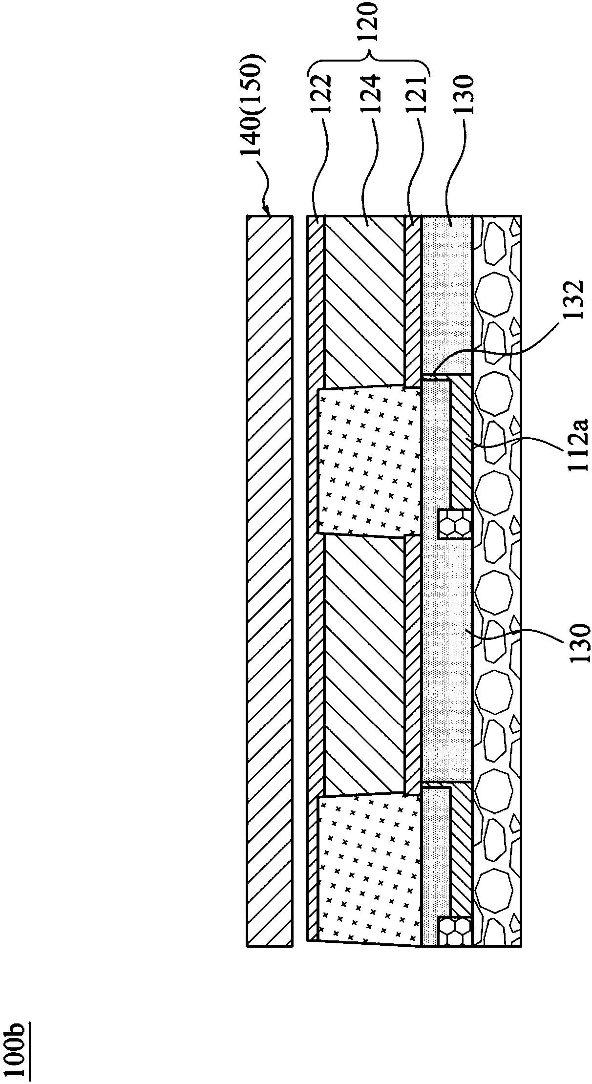
[0034] In order to make the description of the present invention more detailed and complete, the following is an illustrative description of the implementation and specific examples of the present invention; but this is not a limited form of implementing or using the specific implementation of the present invention. The embodiments disclosed below can be combined or substituted for each other when beneficial, and other embodiments or embodiments can also be added to one embodiment or embodiment without further description or illustration. In the following description, many specific details will be described in detail so that those skilled in the art to which the present invention pertains can fully understand the following embodiments. However, embodiments or examples of the invention may be practiced without these specific details. In other instances, well-known structures and devices are only schematically shown in order to simplify the drawings.

[0035] The terms "about",...


PUM


Abstract

An OLED display device includes a substrate, an active element array, at least one OLED, a light absorption layer or an optical scattering layer, and an encapsulation plate. The substrate includes anupper surface and a lower surface opposite to the upper surface. The active element array is configured in the side of the upper surface of the substrate. The OLED are disposed over the active array substrate. The OLED includes a first electrode, a second electrode, and an organic light-emitting layer. The first electrode is disposed in a side adjacent to the active element array, and the second electrode is opposite to the first electrode. Both the first and second electrodes have a high transmittance and a low reflection in a wavelength range of visible light. The organic light-emitting layer is interposed between the first and second electrodes. The light absorption layer or optical scattering layer is disposed between the OLED and the substrate. The encapsulation plate is disposed overthe second electrode. Thus, the OLED display device can solve the problem of reflection of ambient light to creation extent, and the light emitting efficiency of the OLED display device can be improved.

Description

technical field [0001] The invention relates to an organic light emitting diode display device. Background technique [0002] Organic light-emitting diode display panels are regarded as the mainstream technology of the next generation. In a general organic light emitting diode display panel, when the user uses the organic light emitting diode display under a high-brightness ambient light source, the light reflected by the panel from the outside will seriously affect the display screen of the original display, causing the user to be unable to see the original display clearly. display screen. [0003] In traditional organic light emitting diode displays, in order to improve light extraction efficiency, materials with high reflectivity are used as the driving electrodes of organic light emitting diodes, so that the light emitted to the bottom can be reflected by the driving electrodes below, thereby obtaining higher light extraction efficiency . In addition, some people have...

Claims


Application Information

Patent Timeline
IPC IPC(8): H01L27/32H01L51/52H01L51/50
CPCH10K59/00H10K50/11H10K50/805H10K59/40H10K59/124H10K50/816H10K50/828H10K50/854H10K50/865H10K2102/331H10K59/50H10K59/12H10K50/8426H10K59/38
Inventor 刘振宇龚立伟林熙乾
Owner TRENDON TOUCH TECHNOLOGY CORPORATION
Why Eureka
Try Eureka