Display panel testing device and display device

A technology of display panel and test device, applied in static indicators, instruments, etc., can solve problems such as affecting the display results of the display panel

Inactive Publication Date: 2019-02-26
HKC CORP LTD
View PDF5 Cites 1 Cited by
  • Summary
  • Abstract
  • Description
  • Claims
  • Application Information

AI Technical Summary

Problems solved by technology

[0003] However, before bonding the driver chip and the display panel, it is necessary to laser off the shorting bar and the wiring in the connection area (the bridge where the signal generated by the Gate IC reaches the glass end), if there are more than two wires after laser If the wiring is short-circuited, there will be G dark lines, which will affect the display results of the display panel.

Method used


Image

  • Display panel testing device and display device
  • Display panel testing device and display device
  • Display panel testing device and display device

Examples


Embodiment Construction

[0033] It should be understood that the specific embodiments described here are only used to explain the present invention, not to limit the present invention.

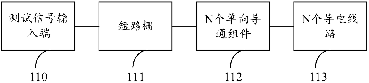
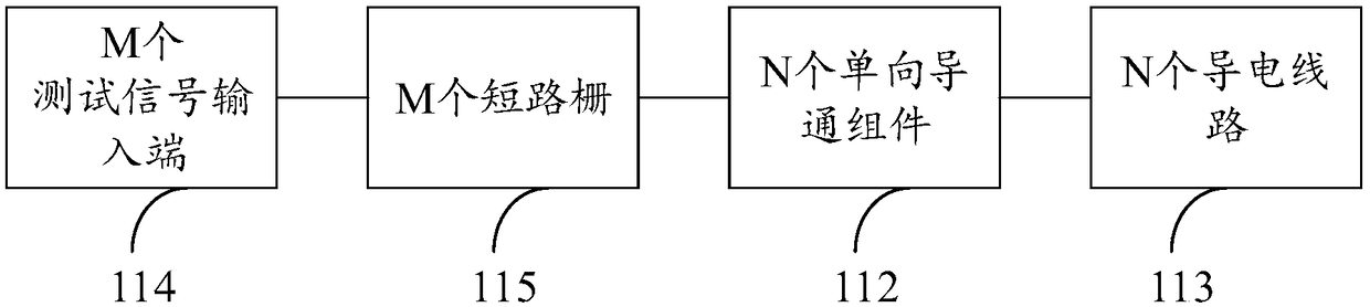
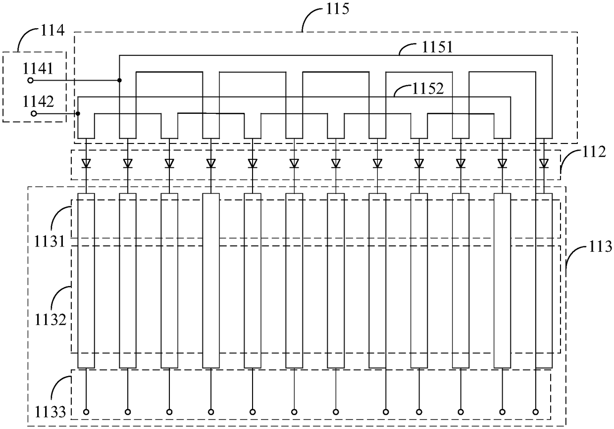
[0034] The technical solutions in the embodiments of the present invention will be clearly and completely described below in conjunction with the accompanying drawings in the embodiments of the present invention. Obviously, the described embodiments are only two parts of the embodiments of the present invention, not all of them. . Based on the embodiments of the present invention, all other embodiments obtained by persons of ordinary skill in the art without creative efforts fall within the protection scope of the present invention.

[0035] It should be noted that all directional indications (such as up, down, left, right, front, back...) in the embodiments of the present invention are only used to explain the relationship between the components in a certain two specific postures (as shown in the accompanying drawing...


PUM


Abstract

The invention discloses a display panel testing device and a display device. The display panel testing device comprises a testing signal input end, a shortcircuit gate, N unidirectional conduction assemblies and N conductive lines. A display panel testing signal which is input through the testing signal input end successively passes the shortcircuit gate, the unidirectional conduction assmelbies and the N conductive lines and is output to a display panel, thereby testing the display panel. The display panel testing device and the display device settle a problem of mutual interference of G concealed lines of the display panel in prior art.

Description

technical field [0001] The invention relates to the technical field of display devices, in particular to a display panel testing device and a display device. Background technique [0002] In the production process of the existing display panel (TFT-LCD), there will be a shorting bar testing (Shorting BarTesting) program, the testing principle is to inject a test signal into the test circuit of the display panel to light up the panel, and generate some Simple test screen, if there are defects on the panel (such as black dots, colored dots, dashed lines and uneven gray levels, etc.), the defects will be displayed on these screens, and then the defective panels will be detected by manual or automatic defect detection system to ensure Unqualified products do not enter the next IC binding process, avoid unnecessary waste of driver chips (IC) and anisotropic conductive film (ACF) and other materials, improve the pass rate of display panel products, and reduce material consumption ...

Claims


Application Information

Patent Timeline
Patent Type & Authority Applications(China)
IPC IPC(8): G09G3/00
CPCG09G3/006
Inventor 单剑锋
Owner HKC CORP LTD
Why Eureka
Try Eureka