Display substrate, display panel, and manufacturing method of display substrate

A display substrate and manufacturing method technology, applied to semiconductor devices, electrical components, circuits, etc., can solve problems such as difficult to achieve display effects, limited electrical compensation effects, etc.

Active Publication Date: 2022-07-29
BOE TECH GRP CO LTD
View PDF3 Cites 0 Cited by
  • Summary
  • Abstract
  • Description
  • Claims
  • Application Information

AI Technical Summary

Problems solved by technology

The commonly used compensation method is electrical compensation, but the effect of electrical compensation is very limited, and it is difficult to further improve the display effect

Method used


Image

  • Display substrate, display panel, and manufacturing method of display substrate
  • Display substrate, display panel, and manufacturing method of display substrate
  • Display substrate, display panel, and manufacturing method of display substrate

Examples


Embodiment Construction

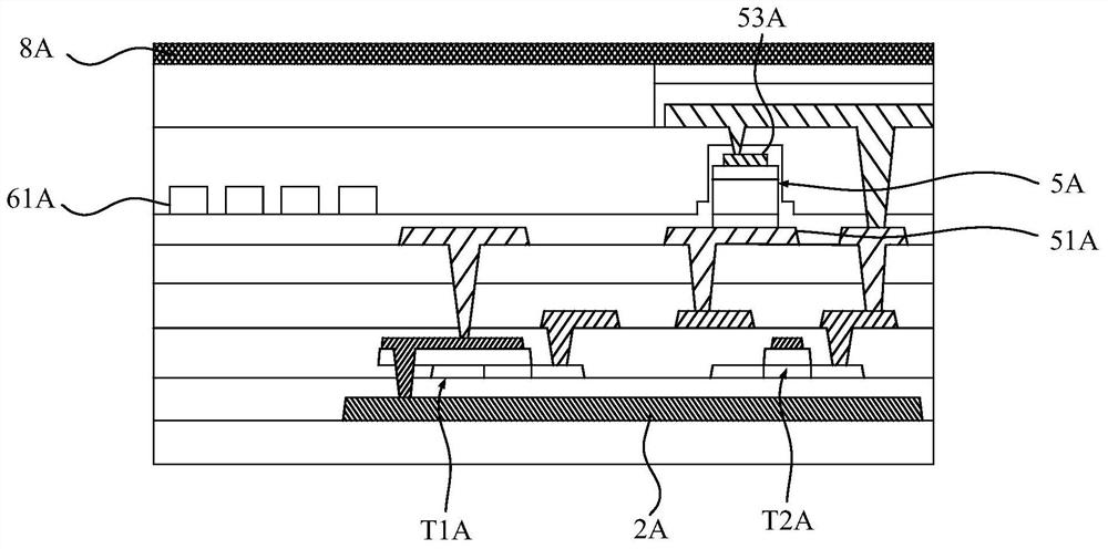
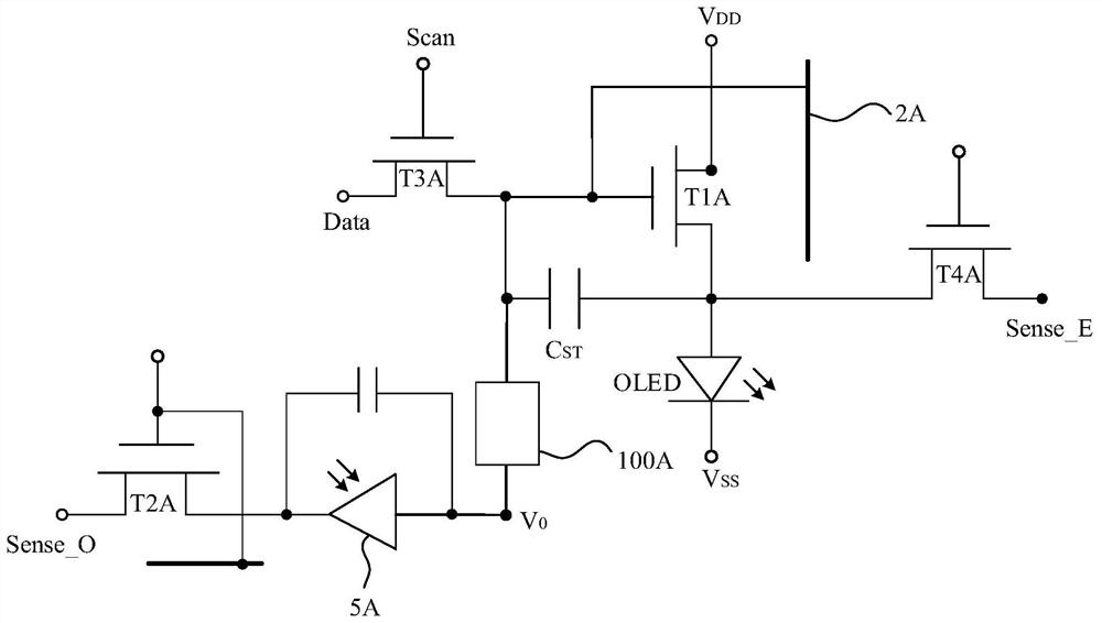
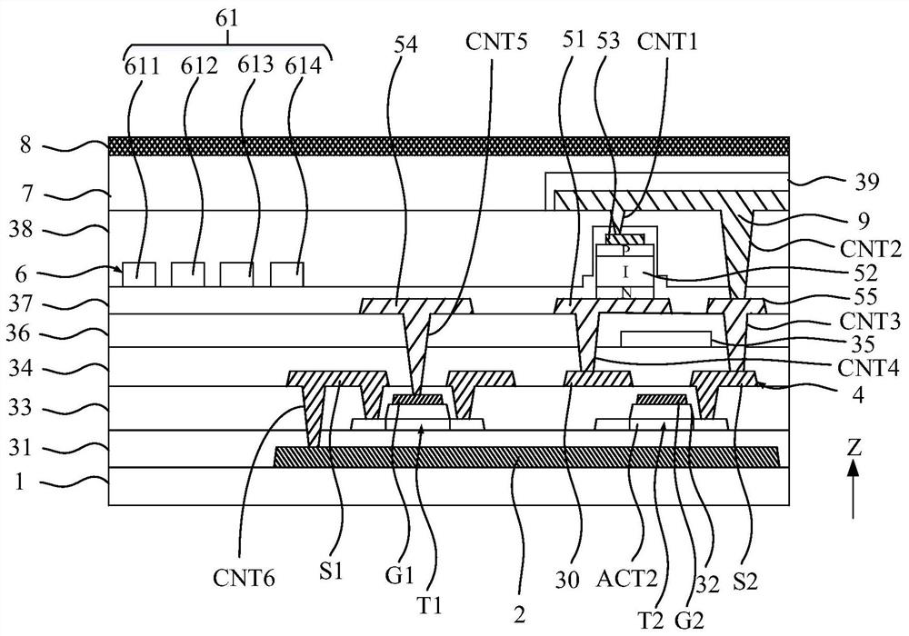
[0028] Exemplary embodiments will be described in detail herein, examples of which are illustrated in the accompanying drawings. Where the following description refers to the drawings, the same numerals in different drawings refer to the same or similar elements unless otherwise indicated. The embodiments described in the following exemplary embodiments are not intended to represent all embodiments consistent with the present invention. Rather, they are merely examples of means consistent with some aspects of the invention as recited in the appended claims.

[0029] The terms used in the present invention are for the purpose of describing particular embodiments only and are not intended to limit the present invention. Unless otherwise defined, technical or scientific terms used in the present invention should have the ordinary meaning as understood by one of ordinary skill in the art to which the present invention belongs. The terms "first", "second" and similar terms used i...


PUM


Abstract

The invention provides a display substrate, a display panel and a method for manufacturing the display substrate. The display substrate includes a substrate, a metal light shielding layer on the substrate; a first thin film transistor, a photodiode and a second thin film transistor on the metal light shielding layer , the output end of the first thin film transistor is electrically connected to the pixel electrode, the photodiode includes a first electrode, a second electrode and a photosensitive layer, and the second electrode of the photodiode is connected to the second thin film transistor to transmit the photocurrent generated by the photodiode To the second thin film transistor; the output end of the first thin film transistor is electrically connected to the metal light shielding layer, and the gate of the first thin film transistor is electrically connected to the first electrode. Since the first electrode is connected to the gate of the first thin film transistor, and the metal light shielding layer is electrically connected to the source of the first thin film transistor, the voltages of the upper and lower layers of the double-gate structure are different, which is beneficial to reduce the effect of hydrogen on the channel of the lower layer. Influenced by the area, an array backplane with better characteristics can be obtained.

Description

technical field [0001] The present invention relates to the field of display, and in particular, to a display substrate, a display panel and a manufacturing method of the display substrate. Background technique [0002] OLED (Organic Light-Emitting Diode, Organic Light Emitting Diode) display technology has the advantages of low power consumption, fast response speed, wide viewing angle, thin thickness, and flexibility. Currently, OLED displays are widely used. In order to improve the display effect of the OLED display panel, the OLED display panel needs to be compensated according to the display state. A commonly used compensation method is electrical compensation, but the effect of electrical compensation is very limited, and it is difficult to further improve the display effect. SUMMARY OF THE INVENTION [0003] In order to solve the above technical problems, the present invention provides a display substrate capable of realizing optical compensation, a display panel a...

Claims


Application Information

Patent Timeline
Patent Type & Authority Patents(China)
IPC IPC(8): H01L27/12H01L27/32
CPCH01L27/1214H01L27/1259H01L27/124H10K59/123H01L29/78633H10K59/126H10K59/13H10K59/131H10K59/88H10K71/60H10K59/1213
Inventor 贺家煜宁策李正亮胡合合黄杰姚念琦
Owner BOE TECH GRP CO LTD
Why Eureka
Try Eureka