Display panel, manufacturing method thereof, and display device

A technology of a display panel and a manufacturing method, which is applied in the fields of display panels and their manufacturing, and display devices, can solve the problems of high manufacturing cost and complicated manufacturing process of display panels.

Active Publication Date: 2019-12-31
BOE TECH GRP CO LTD
View PDF5 Cites 0 Cited by
  • Summary
  • Abstract
  • Description
  • Claims
  • Application Information

AI Technical Summary

Problems solved by technology

[0005] In order to solve the problem that the manufacturing process of the display panel is relatively complicated and the manufacturing cost is high, the present invention provides a display panel, a manufacturing method thereof, and a display device

Method used


Image

  • Display panel, manufacturing method thereof, and display device
  • Display panel, manufacturing method thereof, and display device
  • Display panel, manufacturing method thereof, and display device

Examples


Embodiment Construction

[0085] In order to make the object, technical solution and advantages of the present invention clearer, the implementation manner of the present invention will be further described in detail below in conjunction with the accompanying drawings.

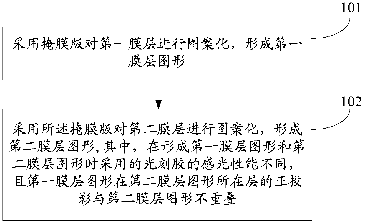
[0086] An embodiment of the present invention provides a method for manufacturing a display panel, the display panel includes a first film layer and a second film layer, such as figure 1 As shown, the method includes:

[0087] Step 101, using a mask to pattern the first film layer to form a pattern of the first film layer.

[0088] Step 102 , using the mask to pattern the second film layer to form a pattern of the second film layer.

[0089] Wherein, the photosensitivity of the photoresist used when forming the first film pattern and the second film pattern is different, and the orthographic projection of the first film pattern on the layer where the second film pattern is located is different from that of the second film pattern. ov...


PUM


Abstract

The invention discloses a display panel, a manufacturing method thereof, and a display apparatus, and belongs to the display technology field. The display panel comprises a first membrane layer and a second membrane layer. The manufacturing method comprises the following steps: using a mask to form patterns on the first membrane layer so as to obtain a first membrane pattern; and using the mask to form patterns on the second membrane layer so as to obtain a second membrane pattern; wherein the photosensitive properties of the photoresists used in the first membrane pattern and the second membrane pattern are different, so the orthographic projection of the first membrane pattern on the second membrane layer is not overlapped on the second membrane pattern. The provided manufacturing method solves the problems that in the prior art the manufacturing technology of display panel is complicated and the manufacture cost is high, simplifies the production process, and reduces the manufacture cost, and the produced display panel can be used to produce display apparatus.

Description

technical field [0001] The present invention relates to the field of display technology, in particular to a display panel, a manufacturing method thereof, and a display device. Background technique [0002] The display panel of the liquid crystal display includes a color filter substrate, an array substrate, and a liquid crystal layer located between the color filter substrate and the array substrate. Mask plates are often used in the process of manufacturing color filter substrates and array substrates. [0003] In the related art, when forming a black matrix pattern on a color filter substrate, the photoresist is first coated on the base substrate, and then a light source is used to irradiate the mask plate, and the light transmitted through the mask plate makes the light on the base substrate The photoresist is photosensitive, and then the photosensitive photoresist is dissolved by developing technology, and the unphotosensitive photoresist is cured. Finally, the process...

Claims


Application Information

Patent Timeline
Patent Type & Authority Patents(China)
IPC IPC(8): G03F7/00G02F1/1335G02F1/1339G02F1/1333
Inventor 李会崔贤植
Owner BOE TECH GRP CO LTD
Why Eureka
Try Eureka