Semiconductor device and method for fabricating the same

a semiconductor and semiconductor technology, applied in the field of field effect semiconductor devices, can solve the problems of difficult to form a via hole penetrating the substrate of the semiconductor device, the thinned substrate becomes brittle, and the device is used, and achieves the effect of high breakdown voltage and facilitate formation of the via hol

Active Publication Date: 2006-03-23
PANASONIC CORP
View PDF3 Cites 69 Cited by
  • Summary
  • Abstract
  • Description
  • Claims
  • Application Information

AI Technical Summary

Benefits of technology

[0013] With the foregoing in mind, an object of the present invention is to provide a semiconductor device contai

Problems solved by technology

The known semiconductor device using a via hole, however, has the following problems.
Therefore, it is extremely difficult to form a via hole penetrating this substrate with the strength of the substrate maintained, that is, with the substr

Method used


Image

  • Semiconductor device and method for fabricating the same
  • Semiconductor device and method for fabricating the same
  • Semiconductor device and method for fabricating the same

Examples


first embodiment

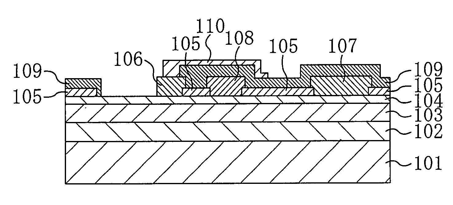
[0040]FIG. 1 is a sectional view schematically showing the structure of a hetero-junction field effect transistor (HFET) according to a first embodiment of the present invention. Referring to FIG. 1, the HFET of the first embodiment includes a p+-type conductive substrate 101, a buffer layer 102, a channel layer 103, and a Schottky layer 104. The p+-type conductive substrate 101 is made of, for example, silicon (Si) and has a thickness of 500 μm. The buffer layer 102 with a thickness of 500 nm is made of aluminum gallium nitride (AlxGa1-xN (0≦x≦1)) of high resistance and provided on the conductive substrate 101. The channel layer 103 with a thickness of 1000 nm is made of undoped gallium nitride (GaN) and provided on the buffer layer 102. The Schottky layer 104 with a thickness of 25 nm is made of n-type aluminum gallium nitride (AlyGa1-yN (0≦y≦1)) and provided on the channel layer 103. The buffer layer 102 is formed to relax the lattice mismatch between the conductive substrate 101...

second embodiment

Modification of Second Embodiment

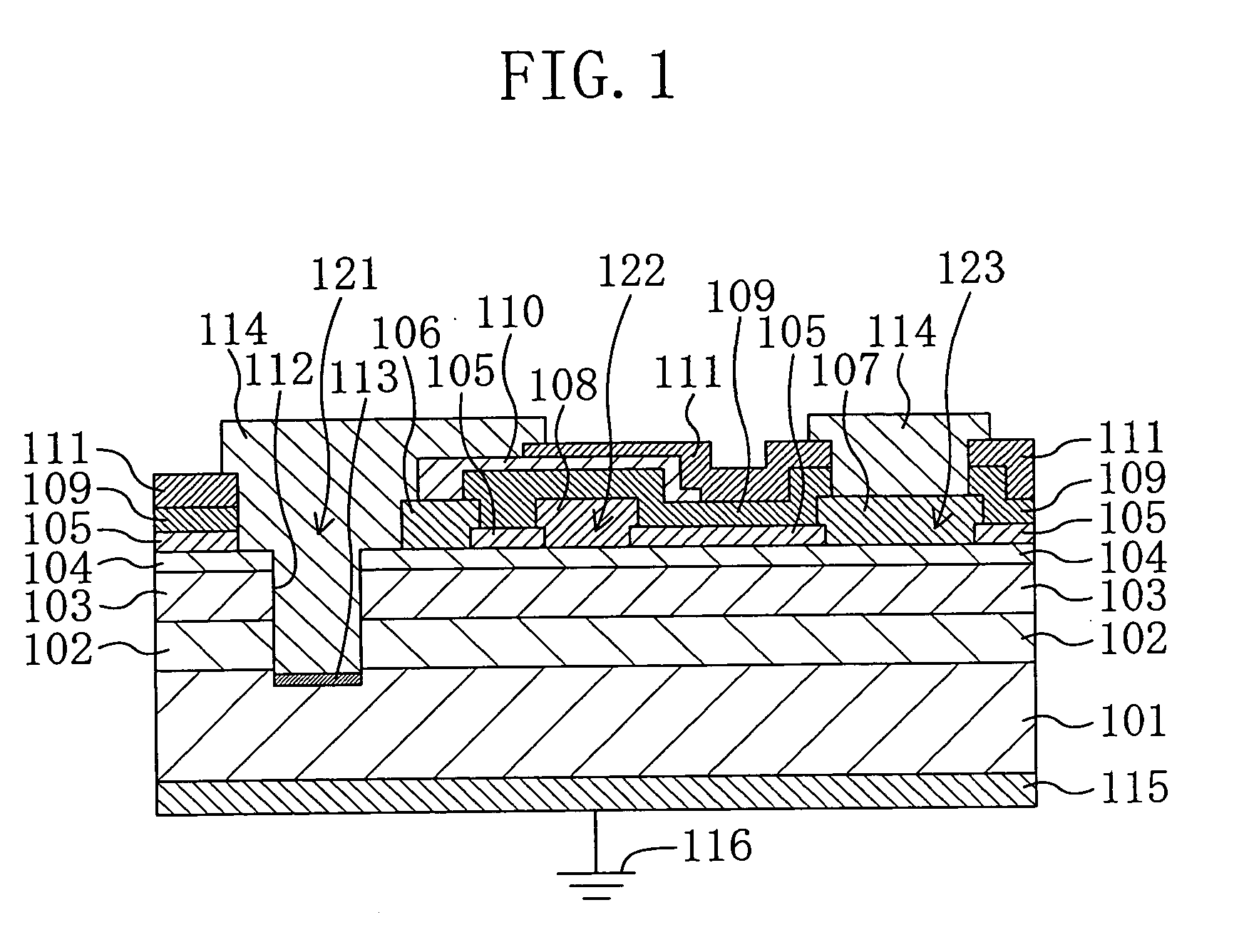
[0069]FIG. 6 is a sectional view schematically showing the structure of a semiconductor device according to a modification of the second embodiment. Referring to FIG. 6, the HFET of this modification includes a semiconductor substrate (or an insulator substrate) 300, a conductive layer 301, a buffer layer 302, a channel layer 303, and a Schottky layer 304. The semiconductor substrate 300 is made of, for example, Si and has a thickness of 500 μm. The 500 nm-thick conductive layer 301 of a low resistance (the resistivity is 0.01 Ωcm or lower) is made of n-type doped Si and provided on the semiconductor substrate 300. The 500 nm-thick buffer layer 302 of a high resistance is made of aluminum gallium nitride (AlxGa1-xN (0≦x≦1)) and provided on the conductive layer 301. The channel layer 303 is made of undoped gallium nitride (GaN) and provided on the buffer layer 302. The Schottky layer 304 with a thickness of 25 nm is made of n-type aluminum gallium nit...


PUM


Abstract

In the structure of a semiconductor device of the present invention, a first source electrode is connected to a conductive substrate through a via hole, and a second source electrode is formed. Thus, even if a high reverse voltage is applied between a gate electrode and a drain electrode, electric field concentration likely to occur at an edge of the gate electrode closer to the drain electrode can be effectively dispersed or relaxed. Moreover, the conductive substrate is used as a substrate for forming element formation layers, so that a via hole penetrating the substrate to reach the backside thereof does not have to be formed in the conductive substrate. Thus, with the strength necessary for the conductive substrate maintained, the first source electrode can be electrically connected to a backside electrode.

Description

CROSS-REFERENCE TO RELATED APPLICATIONS [0001] This application claims priority under 35 U.S.C. § 119 on Patent Application No. 2004-270925 filed in Japan on Sep. 17, 2004, the entire contents of which are hereby incorporated by reference. BACKGROUND OF THE INVENTION [0002] (a) Fields of the Invention [0003] The present invention relates to semiconductor devices made of III-V nitride semiconductor. In particular, the present invention relates to field effect semiconductor devices having high breakdown voltage and to methods for fabricating such a device. [0004] (b) Description of Related Art [0005] III-V nitride semiconductors, that is, mixed crystals represented by the general formula AlxGa1-x-yInyN (where 0≦x≦1, 0≦y≦1) such as gallium nitride (GaN), aluminum nitride (AlN), and indium nitride have, as physical characteristics, wide band gaps and direct transition type band structures. Owing to these characteristics, consideration is being taken of application of the III-V nitride s...

Claims


Application Information

Patent Timeline
IPC IPC(8): H01L31/112H01L29/20H01L29/80
CPCH01L29/2003H01L29/402H01L29/7787H01L29/41766H01L29/4175
Inventor HIKITA, MASAHIROUENO, HIROAKIHIROSE, YUTAKAYANAGIHARA, MANABUUEMOTO, YASUHIROTANAKA, TSUYOSHI
Owner PANASONIC CORP
Why Eureka
Try Eureka