Insulated Gate Semiconductor Device and Method for Producing the Same

a technology of semiconductor devices and gate semiconductors, which is applied in the direction of semiconductor devices, basic electric elements, electrical equipment, etc., can solve the problems of lowering the breakdown voltage and unable to obtain predetermined breakdown voltages, and achieves the effect of increasing the breakdown voltage of the terminal area, facilitating the connection of depletion layers, and increasing the resistan

Active Publication Date: 2008-04-17
DENSO CORP +1
View PDF15 Cites 76 Cited by
  • Summary
  • Abstract
  • Description
  • Claims
  • Application Information

AI Technical Summary

Benefits of technology

[0020] It is further preferable that the pitches of the respective trench portions in the second trench portion group of the insulation gate type semiconductor device according to the invention are narrower than those of the respective trench portions in the first trench portion group. That is, since the terminal area in which the second trench portion group is provided is an inactive area, no drift current flows. Therefore, there is no case where the ON resistance is increased even if the interval between the second floating regions is made narrow. Therefore, by narrowing the pitches of the respective trench portions in the second trench portion group, that is, narrowing the interval between the second floating regions, it becomes easier for the depletion layers to be connected, wherein higher breakdown voltage of the terminal area can be obtained.
[0021] Also, in the insulation gate type semiconductor device according to the invention, it is preferable that the trench portion which is positioned inward is made deeper than the trench portions adjacent to each other in the second trench portion group. That is, by making gradually shallower the depth of the respective trench portions in the second trench portion group from inward to outward, the curvature of the tip end portion of the depletion layer can be reduced. Therefore, higher breakdown voltage of the terminal area can be achieved.
[0022] Further, in the insulation gate type semiconductor device according to the invention, it is preferable that the depth of the respective trench portions in the second trench portion group is made deeper than the depth of the respective trench portions in the first trench portion group. That is, since the terminal area is an inactive area, no breakdown current flows. Therefore, if any insulation breakage occurs in the terminal area, there is a fear that a device is broken down. Therefore, the depth of the respective trench portions in the second trench portion group is made deeper than the depth of the respective trench portions in the first trench portion group. That is, by making the position of the second floating region deeper than the position of the first floating region, the thickness of the depletion spread in the terminal area is made thicker than the thickness of the cell area, whereby the terminal area is made into higher breakdown voltage than in the cell area, and it is possible to prevent insulation breakdown in the terminal area.
[0023] Also, in the insulation gate type semiconductor device described above, it is preferable that the groove width of the respective trench portions in the second trench portion group is made wider than the groove width of the respective trench portions in the first trench portion group. That is, since the widths of the trench portions differ from each other, etching is carried out to a deeper groove position by a micro−loading effect in the trenches, whose groove width is wider, even if the etching is carried out under the same conditions. Further, since the groove width is wide, the size of the floating region formed downward of the respective trench portions is made larger. Therefore, only by making the groove of the trenches wider when executing patterning, the position of the second floating region can be made deeper.
[0024] Also, in the insulation gate type semiconductor device according to the invention, it is further preferable that the end portion of the body region in the plate surface direction is positioned further inward of the outermost trench portion, which is positioned extremely outward, in the second trench portion group. That is, by the end portion of the body region in the plate surface direction being positioned further inward of the outermost trench portion, the depletion layer spread in the plate surface direction from the boundary phase with the body region is interrupted by the wall surface of the trench portion in the second trench portion group. For this reason, it is possible to reduce the size of the terminal area, and compactness of the entirety of the semiconductor device can be achieved.

Problems solved by technology

However, there are the following problems in the insulation gate type semiconductor device 900 described above.
As a result, there may be a case where the breakdown voltage is lowered.
That is, the depletion layers are different from each other in regard to the spread, wherein there may be cases where predetermined breakdown voltage cannot be obtained.

Method used


Image

  • Insulated Gate Semiconductor Device and Method for Producing the Same
  • Insulated Gate Semiconductor Device and Method for Producing the Same
  • Insulated Gate Semiconductor Device and Method for Producing the Same

Examples


Embodiment Construction

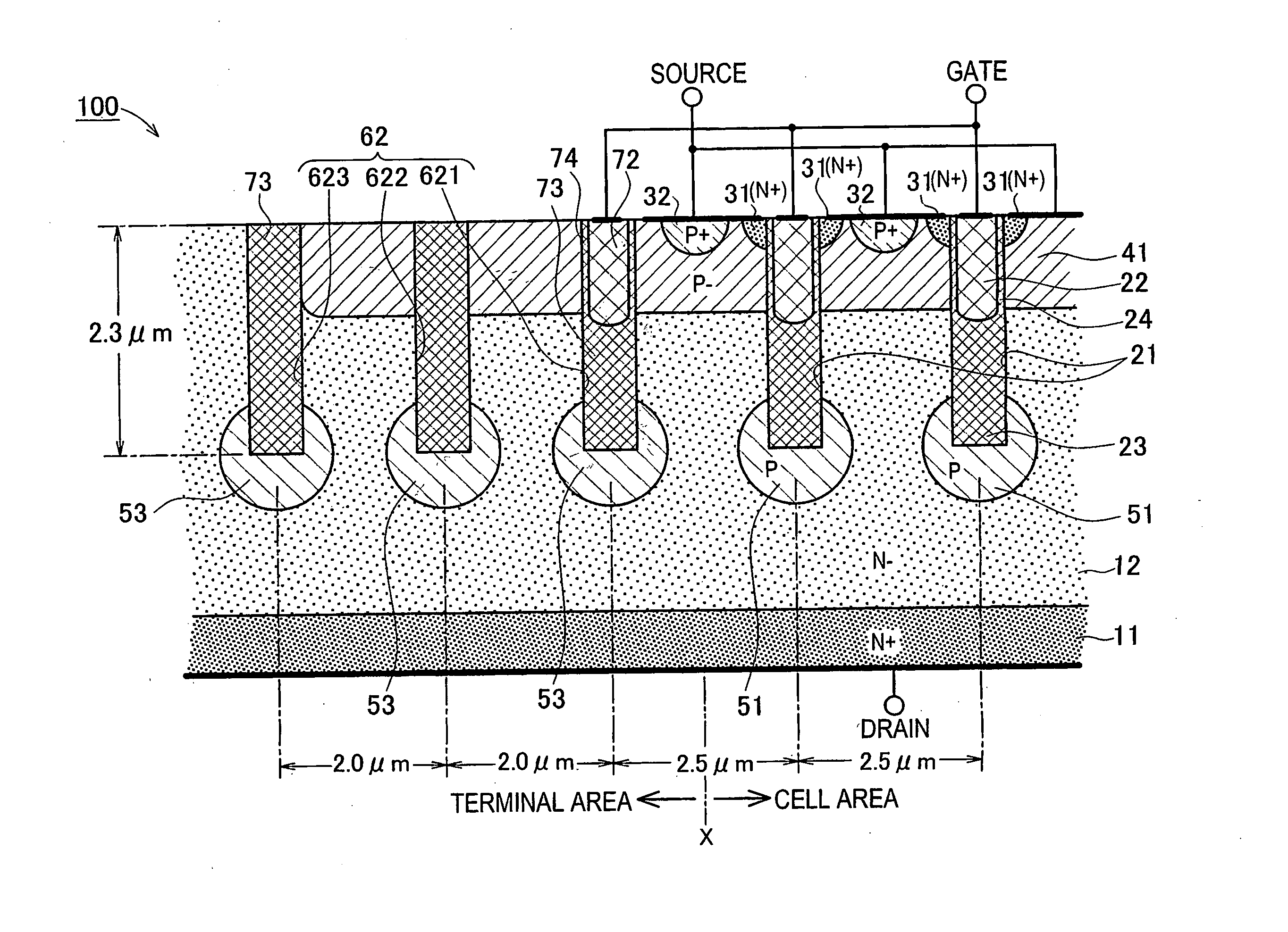
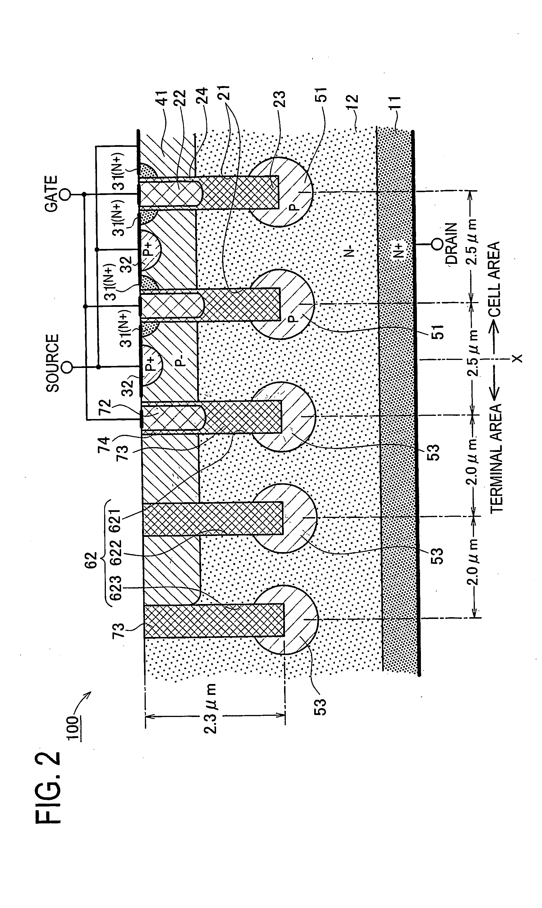
[0043] Hereinafter, a detailed description is given of an embodiment in which the invention, with reference to the accompanying drawings. Also, the present embodiment is such that the invention is applied to a power MOS of controlling conductivity between the drain and source (D and S) by voltage application to an insulation gate.

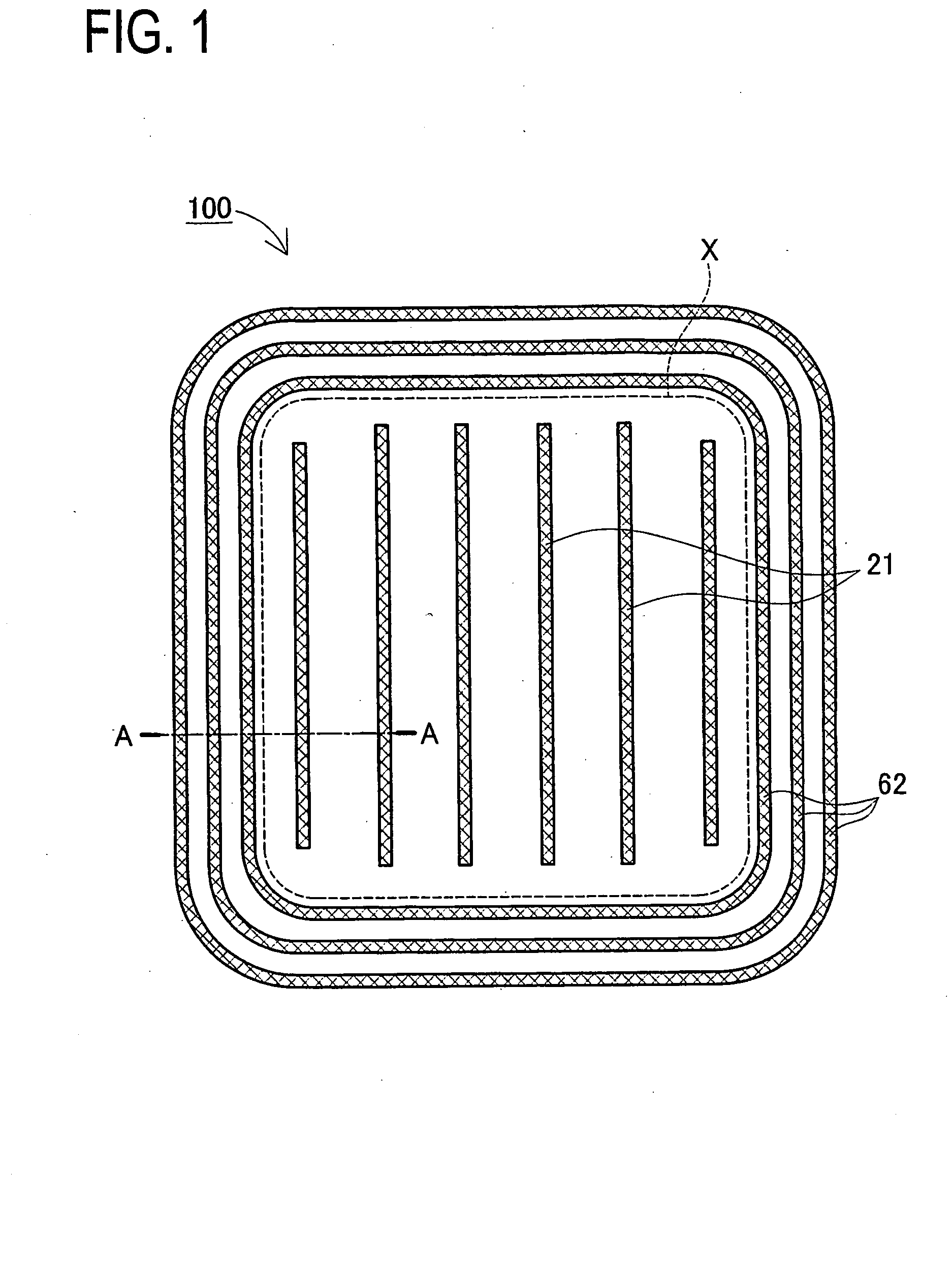
[0044] An insulation gate type semiconductor device 100 (hereinafter called a “semiconductor device 100”) according to the embodiment has a structure shown in a plan perspective view of FIG. 1 and a sectional view of FIG. 2. Also, it is assumed, in the present description, that the entirety in which a starting substrate and a portion of single crystal silicon formed by epitaxial growth on the starting substrate are combined is called a “semiconductor substrate.”

[0045] A semiconductor device 100 of this mode is composed of a cell area (inside the broken line X in FIG. 1) in which a current flows as shown in FIG. 1 and a terminal area (outside the broken lin...


PUM


Abstract

The invention has an object to provide an insulation gate type semiconductor device and a method for producing the same in which high breakdown voltage and compactness are achieved. The semiconductor device has a gate trench and a P floating region formed in the cell area and has a terminal trench and a P floating region formed in the terminal area. In addition, a terminal trench of three terminal trenches has a structure similar to that of the gate trench, and the other terminal trenches have a structure in which an insulation substance such as oxide silicon is filled. Also, the P floating region 51 is an area formed by implanting impurities from the bottom surface of the gate trench, and the P floating region is an area formed by implanting impurities from the bottom surface of the terminal trench.

Description

[0001] This is a 371 national phase application of PCT / JP2005 / 018406 filed 28 Sep. 2005, which claims priority of Japanese Patent Application No. 2004-316912 filed 29 Oct. 2004, the contents of which are incorporated herein by reference.FIELD OF THE INVENTION [0002] The present invention relates to an insulation gate type semiconductor device having a trench gate structure. In particular, the invention relates to an insulation gate type semiconductor device having floating regions beneath trenches and capable of securely achieving high breakdown voltage by relieving an electric field applied to a semiconductor layer. BACKGROUND OF THE INVENTION [0003] Conventionally, a trench gate type semiconductor device having a trench gate structure has been proposed as an insulation gate type semiconductor device for a power device. In the trench gate type semiconductor device, generally, high breakdown voltage and low on resistance are in the relationship of trade-off. [0004] The present appli...

Claims


Application Information

Patent Timeline
Patent Type & Authority Applications(United States)
IPC IPC(8): H01L29/78H01L21/336
CPCH01L29/0623H01L29/402H01L29/7813H01L29/42368H01L29/407H01L29/4238H01L29/66734H01L29/7811H01L29/0653
Inventor TAKAYA, HIDEFUMIHAMADA, KIMIMORIMIYAGI, KYOSUKEOKURA, YASUSHIKUROYANAGI, AKIRATOKURA, NORIHIKO
Owner DENSO CORP
Why Eureka
Try Eureka