Ic chip mounting substrate, ic chip mounting substrate manufacturing method, optical communication device, and optical communication device manufacturing method

a technology of ic chip and mounting substrate, which is applied in the direction of circuit optical details, non-printed circuit electric components association, non-metallic protective coating application, etc., can solve the problems of large size of the device itself, difficult to make the terminal device small in size, and difficult to make a fine adjustment for alignment, etc., to achieve excellent connection reliability, small in size, excellent reliability

Inactive Publication Date: 2006-01-19
IBIDEN CO LTD
View PDF25 Cites 251 Cited by
  • Summary
  • Abstract
  • Description
  • Claims
  • Application Information

AI Technical Summary

Benefits of technology

[0050] Further, as a result of the dedicated study, the present inventors found that by disposing the substrate for mounting an IC chip on which various optical components are mounted and the multilayered printed circuit board to be confronting each other, it is possible to realize optical communication excellent in connection reliability and contribute to making the terminal device small in size, and completed a device for optical communication having the following configuration according to the first aspect of the third group of the present invention, a device for optical communication having the following configuration according to the first aspect of the fourth group of the present invention and also completed manufacturing methods of the devices for optical communication.
[0051] Moreover, the present inventors found that when a sealing resin layer is formed between the substrate for mounting an IC chip and the multilayered printed circuit board that are disposed to be confronting each other in the device for optical communication, it is possible to prevent the foreign matters and the like floating in the air from entering between the respective optical components and moderate the stress generated between the substrate for mounting an IC chip and the multilayered printed circuit board, thereby ensuring a device for optical communication excellent in reliability.

Problems solved by technology

When the package substrate having an IC chip mounted thereon, optical elements, such as a light receiving element and a light emitting element, which process optical signal, and the like are mounted separately on such a conventional terminal device, the size of a device itself becomes large, making it difficult to make the terminal device small in size.
Although such an optical element-internalizing package substrate can solve the problem in that the device itself becomes large in size, this package substrate has the following problems.
In the optical element-internalizng package substrate, since the optical elements are completely internalized inside the substrate, it is difficult to make a fine adjustment for alignment upon connection of the package substrate to an external optical element (e.g., an optical fiber or an optical waveguide).
As can be seen, when positional deviation occurs to the included optical elements, connection loss generated at the time of connecting the package substrate to the external optical component (e.g., an optical waveguide) is large, which deteriorates connection reliability in optical communication.

Method used


Image

  • Ic chip mounting substrate, ic chip mounting substrate manufacturing method, optical communication device, and optical communication device manufacturing method
  • Ic chip mounting substrate, ic chip mounting substrate manufacturing method, optical communication device, and optical communication device manufacturing method
  • Ic chip mounting substrate, ic chip mounting substrate manufacturing method, optical communication device, and optical communication device manufacturing method

Examples


example 1

[1850] A. Manufacturing of Resin Film for Interlaminar Insulating Layer

[1851] 30 parts by weight of Bisphenol A type epoxy resin (epoxy equivalent 469, Epikote 1001 made by Yuka Shell Epoxy Co.), 40 parts by weight of cresol novolak type epoxy resin (epoxy equivalent 215, Epichlon N-673 made by Dainippon Ink and Chemicals, Inc.), and 30 parts by weight of phenol novolak resin containing triazine structure (phenolic hydroxy equivalent 120, Phenolite KA-7052 made by Dainippon Ink and Chemicals, Inc.) were dissolved while being heated in 20 parts by weight of ethyl diglycol acetate and 20 parts by weight of solvent naphtha under stirring condition, followed by the addition of 15 parts by weight of epoxy-terminated polybutadiene rubber (made by Nagase Chemicals Ltd.; Denalex R-45EPT) and 1.5 parts by weight of a pulverized product of 2-phenyl-4,5-bis (hydroxymethyl) imidazole, 2 parts by weight of a finely pulverized silica, and 0.5 parts by weight of a silicone based defoaming agent t...

example 2

[1894] A substrate for mounting an IC chip was obtained similarly to Example 1 except that a resin composition containing polyolefin was employed in place of the resin composition containing epoxy resin in the step (18) of Example 1.

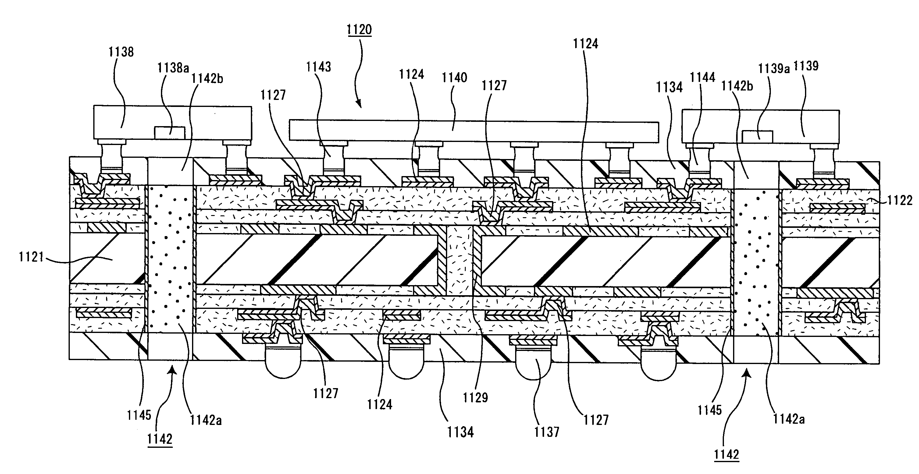
[1895] It is noted that in the substrate for mounting an IC chip manufactured in this example, each of the optical paths for transmitting optical signal is constituted by the resin composition, a vacancy and the conductor layer around them.

example 3

[1896] A substrate for mounting an IC chip was obtained similarly to Example 1 except that the step (18) of Example 1, i.e., the step of forming the resin composition layer 1042a was not executed.

[1897] It is noted that in the substrate for mounting an IC chip manufactured in this example, each of the optical paths for transmitting optical signal is constituted by a vacancy and the conductor layer around the vacancy.


PUM


Abstract

An object of the present invention is to provide a substrate for mounting an IC chip which is a component for optical communication having an IC chip and an optical component integrally provided thereon, which can ensure a short distance between the IC chip and the optical component, which is excellent in electric signal transmission reliability and which can transmit optical signal through an optical path for transmitting optical signal. The substrate for mounting an IC chip of the present invention is a substrate for mounting an IC chip comprising: a substrate and, as serially built up on both faces thereof, a conductor circuit and an interlaminar insulating layer in an alternate fashion and in repetition; a solder resist layer formed as an outermost layer; and an optical element mounted thereto, wherein an optical path for transmitting optical signal, which penetrates the substrate for mounting an IC chip, is disposed.

Description

TECHNICAL FIELD [0001] The present invention relates to a substrate for mounting an IC chip, a manufacturing method of a substrate for mounting an IC chip, a device for optical communication, and a manufacturing method of a device for optical communication. BACKGROUND ART [0002] Recently, attention has been focused on optical fibers mainly in communication fields. Particularly in the IT (Information Technology) field, a communication technique which employs the optical fibers is necessary to provide a high speed Internet network. [0003] The optical fiber has features of (1) low loss, (2) high band, (3) small diameter and light weight, (4) non-induction, (5) resource saving, and the like. A communication system which employs the optical fibers having these features can considerably decrease the number of relays as compared with a communication system which employs conventional metallic cables, can be easily constructed and maintained, and can improve its economical efficiency and rel...

Claims


Application Information

Patent Timeline
Patent Type & Authority Applications(United States)
IPC IPC(8): H05K1/18G02B6/43H05K1/02H05K1/14H05K3/28H05K3/46
CPCG02B6/43H01L24/73H01L2924/12041H01L2924/15311H01L2224/73265H01L2224/32225H01L2224/16225H01L2924/01322H01L2924/01087H01L2924/01074H01L2224/48227H01L2924/01011H01L2924/01012H01L2924/01013H01L2924/0102H01L2924/01029H01L2924/0103H01L2924/01032H01L2924/01033H01L2924/01046H01L2924/01049H01L2924/01058H01L2924/01061H01L2924/01078H01L2924/01079H01L2924/01082H01L2924/01088H01L2924/10329H01L2924/14H01L2924/19041H05K1/0274H05K3/28H05K3/4602H01L2924/01005H01L2924/01006H01L2924/01019H01L2924/01023H01L2924/01024H01L2924/01042H01L2924/01045H01L2924/01047H01L2924/00012H01L2924/00H01L2924/15787H01L2924/15788H01L2924/12042H01L2924/12043H01L2224/05573H01L2224/05568H01L2924/00014H01L2224/05599
Inventor ASAI, MOTOOKODAMA, HIROAKITANAKA, TOYOAKI
Owner IBIDEN CO LTD
Why Eureka
Try Eureka