Multilayer wiring substrate and method of manufacturing the same

a wiring substrate and multi-layer technology, applied in the direction of printed circuit aspects, printed element electric connection formation, conductive pattern formation, etc., can solve the problems of unnecessary portions of plating etching, obstacle to high-density disposition of patterned wiring lines, etc., to prevent delamination, reduce the effect of delamination and preventing delamination

Inactive Publication Date: 2012-06-21
NGK SPARK PLUG CO LTD
View PDF7 Cites 64 Cited by
  • Summary
  • Abstract
  • Description
  • Claims
  • Application Information

AI Technical Summary

Benefits of technology

[0022]The terminal pads receive influences from another wiring substrate or a component connected to the terminal pads, whereby stress concentrates at the terminal pads. Also, a relatively large stress acts on via conductors connected directly to the terminal pads. Therefore, delamination is apt to occur starting from the connections between the via conductors and the interlayer wiring connected directly to the via conductors. In the wiring substrate of the above-described mode, stepped portions are formed in opening verge regions around the via holes such that the stepped portions are depressed from peripheral regions around the opening verge regions. Such stepped portions can disperse the stress acting on the connections between the via conductors and the interlayer wiring, to thereby restrain delamination.
[0023]Preferably, the interlayer wiring is formed on the stepped portions and the peripheral regions, and other via conductors are connected to portions of the interlayer wiring formed on the peripheral regions. Preferably, a thickness of portions of the interlayer wiring formed on the stepped portions of the interlayer insulation layer is greater than a thickness of portions of the interlayer wiring formed on the peripheral regions of the interlayer insulation layer. Since the thickness of the interlayer wiring is increased at the connections between the via conductors and the interlayer wiring, from which delamination is apt to start, delamination can be prevented.
[0024]Preferably, the interlayer wiring includes lands connected to the ends of the via conductors, and the maximum diameters of the lands are equal to or greater than those of the corresponding stepped portions. By virtue of this feature, in the interlayer wiring, the stepped portions are reliably covered with the corresponding lands; thus, delamination can be prevented without fail.
[0025]The connection pads may be pads which are connected to a semiconductor chip via solder bumps. Since the semiconductor chip differs in coefficient of thermal expansion from the wiring substrate, stress is apt to concentration at connections between the semiconductor chip and the wiring substrate. However, in the case where the wiring substrate of the above-described mode is employed, the stress acting on the connections between the connection pads for the semiconductor chip and the interlayer wiring can be dispersed, whereby delamination can be restrained.

Problems solved by technology

; and unnecessary portions of the plating are etched away.
In this case, such a condition is an obstacle to high-density disposition of the patterned wiring lines 102.

Method used


Image

  • Multilayer wiring substrate and method of manufacturing the same
  • Multilayer wiring substrate and method of manufacturing the same
  • Multilayer wiring substrate and method of manufacturing the same

Examples


first embodiment

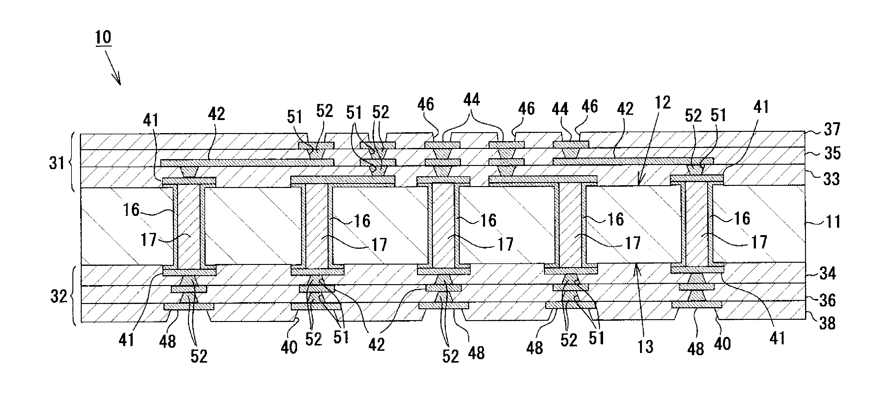
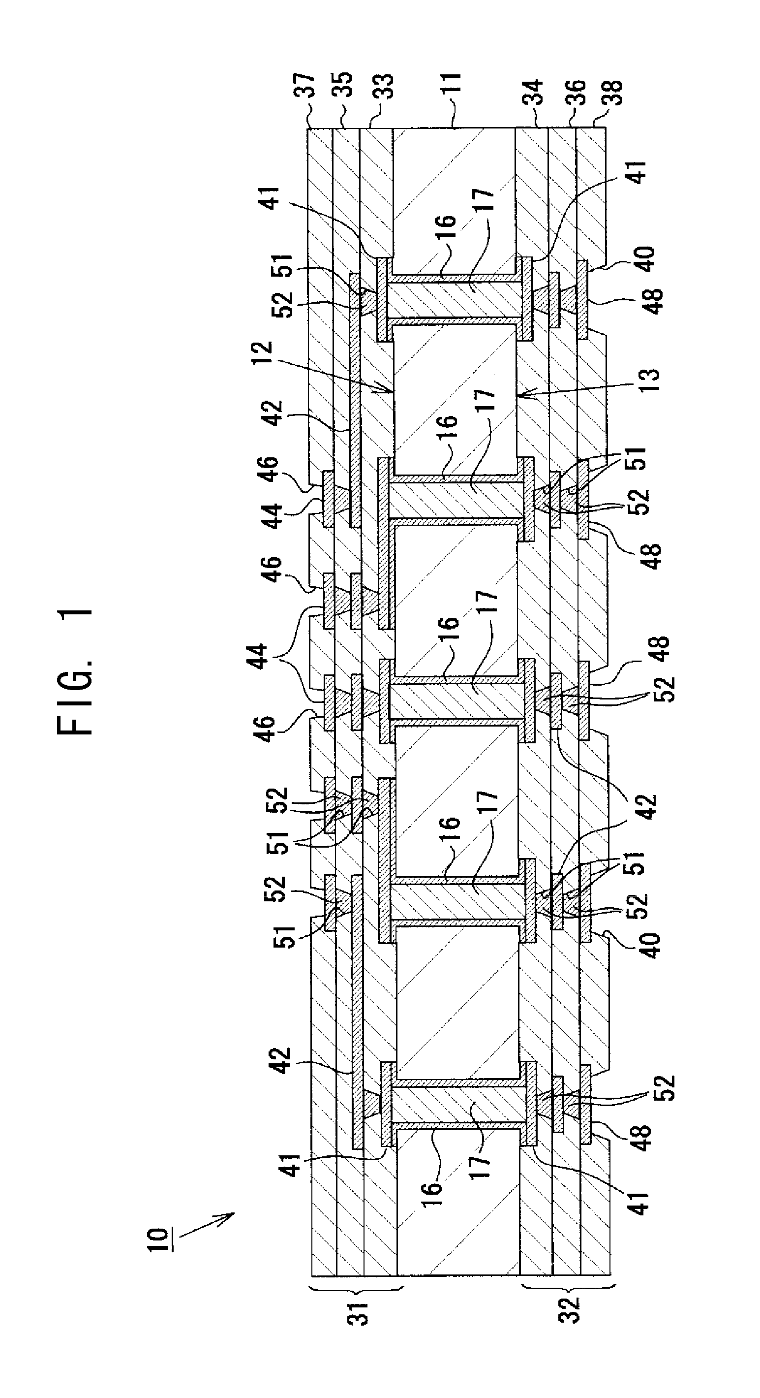
[0047]A multilayer wiring substrate according to a first embodiment of the present invention will next be described in detail with reference to the drawings.

[0048]As shown in FIG. 1, a multilayer wiring substrate 10 of the present embodiment includes a core substrate 11 resembling a substantially square plate; a first buildup layer 31 formed on a core main surface 12 of the core substrate 11; and a second buildup layer 32 formed on a core back surface 13.

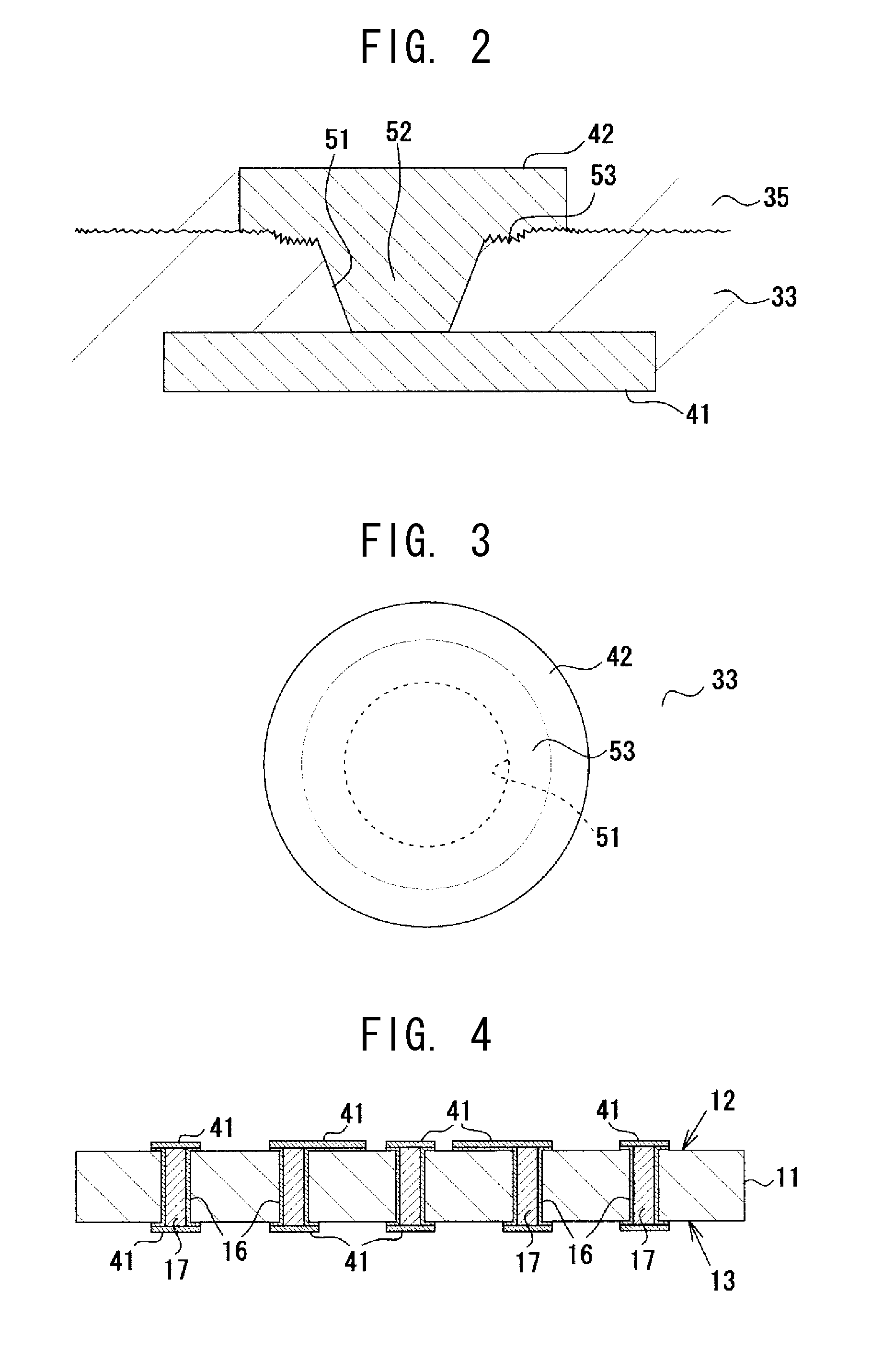
[0049]The core substrate 11 of the present embodiment is a plate having a substantially square shape as viewed in plane and measures 25 mm length×25 mm width×0.9 mm thickness. The core substrate 11 is formed of, for example, a resin insulation material (a glass epoxy material) in which glass cloth serving as a reinforcement material is impregnated with epoxy resin. The core substrate 11 has a plurality of through hole conductors 16 extending therethrough between the core main surface 12 and the core back surface 13. The interiors of...

second embodiment

[0069]The semiconductor package 110 according to a second embodiment of the present invention and a method of manufacturing the same will next be described in detail with reference to the drawings. As shown in FIG. 12, the semiconductor package 110 of the present embodiment is of a BGA (ball grid array) type, and is composed of a multilayer wiring substrate 111 and a IC chip 121 (chip component), which is a semiconductor integrated circuit element. Notably, the type of the semiconductor package 110 is not limited to BGA, and may be PGA (pin grid array), LGA (land grid array), or the like. The IC chip 121 is preferably formed of silicon whose coefficient of thermal expansion is 4.2 ppm / ° C. and assumes the form of a rectangular flat plate whose size is 15.0 mm (length)×15.0 mm (width)×0.8 mm (thickness).

[0070]Meanwhile, the exemplary multilayer wiring substrate 111 does not have a core substrate, and has a wiring stacked portion 140 (laminated structure) composed of conductor layers ...


PUM

PropertyMeasurementUnit
surface roughnessaaaaaaaaaa
depthaaaaaaaaaa
widthaaaaaaaaaa

Abstract

To provide a multilayer wiring substrate in which the connection reliability of via conductors is enhanced, via holes are formed in a resin interlayer insulation layer which isolates a lower conductor layer from an upper conductor layer, and via conductors are formed in the via holes for connecting the lower conductor layer and the upper conductor layer. The surface of the resin interlayer insulation layer is a rough surface, and the via holes open at the rough surface of the resin interlayer insulation layer. Stepped portions are formed in opening verge regions around the via holes such that the stepped portions are recessed from peripheral regions around the opening verge regions. The stepped portions are higher in surface roughness than the peripheral regions.

Description

CROSS REFERENCE TO RELATED APPLICATIONS[0001]The present application claims priority from Japanese Patent Application No. 2010-280320, which was filed on Dec. 16, 2010, and Japanese Patent Application No. 2011-240394, which was filed on Nov. 1, 2011, the disclosures of which are herein incorporated by reference in their entirety.BACKGROUND OF THE INVENTION[0002]1. Field of the Invention[0003]The present invention relates to a multilayer wiring substrate in which via holes are formed in interlayer insulation layers each isolating a lower conductor layer from an upper conductor layer, and via conductors are formed in the respective via holes for connecting the lower conductor layer and the upper conductor layer, as well as to a method of manufacturing the multilayer wiring substrate.[0004]2. Description of Related Art[0005]In recent years, in association with a size reduction in electrical equipment, electronic equipment, etc., a reduction in size, and densification are required of mu...

Claims


Application Information

Patent Timeline
Patent Type & Authority Applications(United States)
IPC IPC(8): H01L23/498H05K1/00H05K3/10H05K1/11
CPCH05K1/115H05K3/0035H05K3/4644H05K3/4682H05K2201/09845H05K2201/09854Y10T29/49155H05K2203/1476H01L23/49822H01L23/49827H01L2224/16225H01L2924/15311H01L23/5226H05K2203/108H01L2224/16227H05K3/40H05K3/46
Inventor MAEDA, SHINNOSUKE
Owner NGK SPARK PLUG CO LTD
Why Eureka
Try Eureka