Carrier-free semiconductor package and fabrication method thereof

Inactive Publication Date: 2008-01-01
SILICONWARE PRECISION IND CO LTD
View PDF10 Cites 77 Cited by
  • Summary
  • Abstract
  • Description
  • Claims
  • Application Information

AI Technical Summary

Benefits of technology

[0019]Therefore, the foregoing coating layers provided on the electrical contacts effectively enhance the bonding strength between the bonding wires and the electrical contacts, such that peel-off of the electrical con

Problems solved by technology

However, in accordance with the development of light-weight and small-profile semiconductor products, the conventional lead frame having a limitation on its thickness makes the height of the lead-frame-based semiconductor package not able to be further reduced, and as a result, a carrier-free semiconductor package structure has been produced.
The above carrier-free semiconductor package advantageously has a reduced thickness, however, it may encounter the problem of delamination of an encapsulant or cracks of bonding wires, etc. due to the absence of the lead frame.
This would cause a delamination problem due to the CTE mismatch and even lead to cracks of the bonding wires 53.
Furthermore, when the semiconductor package is mounted on a printed circuit

Method used


Image

  • Carrier-free semiconductor package and fabrication method thereof
  • Carrier-free semiconductor package and fabrication method thereof
  • Carrier-free semiconductor package and fabrication method thereof

Examples


Embodiment Construction

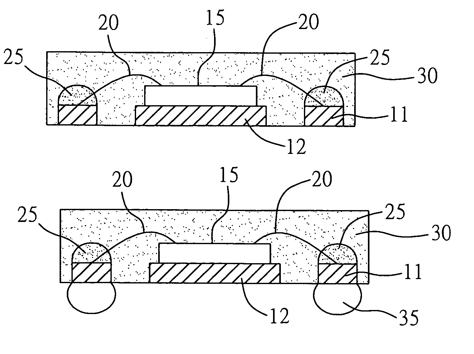
[0026]A fabrication method of a carrier-free semiconductor package proposed in the present invention are described in detail with reference to FIGS. 5A to 5G. First referring to FIG. 5A, a copper carrier 10 is provided, which is patterned to form a die pad 12 thereon and a plurality of electrical contacts 11 around the die pad 12 according to predetermined circuitry. The electrical contacts 11 are thin electroplated pads each comprising such as Au / Pd / Ni / Pd (gold / palladium / nickel / palladium) electroplated layers, so as to satisfy the requirement of profile miniaturization. Then, referring to FIG. 5B, a chip 15 is mounted on the die pad 12 of the carrier 10, and a wire-bonding process is performed to electrically connect the chip 15 to the plurality of electrical contacts 11 via a plurality of bonding wires 20. In order to assure the bonding strength of the bonding wires 20, referring to FIG. 5C, a coating layer 25 is applied on each of the electrical contacts 11 to completely cover th...


PUM


Abstract

A carrier-free semiconductor package and a fabrication method thereof are provided. The fabrication method includes the steps of: providing a carrier having a plurality of electrical contacts formed thereon; mounting at least one chip on the carrier; electrically connecting the chip to the electrical contacts via a plurality of bonding wires; forming a coating layer on each of the electrical contacts to encapsulate a bonded end of each of the bonding wires on the electrical contacts; performing a molding process to form an encapsulant for encapsulating the chip, the bonding wires and the electrical contacts; and removing the carrier, such that bottom surfaces of the electrical contacts are exposed from the encapsulant. This obtains a semiconductor package not having a carrier, and the coating layers can enhance adhesion between the electrical contacts and the encapsulant.

Description

FIELD OF THE INVENTION[0001]The present invention relates to carrier-free semiconductor packages and fabrication methods thereof, and more particularly, to a wire-bonded semiconductor package not having a carrier, and a fabrication method of the semiconductor package.BACKGROUND OF THE INVENTION[0002]For a conventional quad flat non-leaded (QFN) semiconductor package with a lead frame, a plurality of leads surrounding a die pad of the lead frame are usually formed with stepped structures or anchoring structures. As shown in FIGS. 1A, 1B and 1C, the stepped structures 41 of the leads 40 in FIG. 1B or the anchoring structures 42 of the leads 40 in FIG. 1C can increase a contact area between an encapsulant 43 and the leads 40 and thus enhance the adhesion therebetween. Such arrangement prevents delamination of the leads 40 or encapsulant 43, and also provides protection for a chip 44 and bonding wires 45 incorporated in the semiconductor package, thereby assuring the structural reliabil...

Claims


Application Information

Patent Timeline
IPC IPC(8): H01L21/44H01L21/48H01L21/50H01L23/48H01L23/495H01L23/498H01L23/52
CPCH01L21/568H01L23/3107H01L23/3128H01L2224/48091H01L2224/48465H01L2224/48997H01L2224/85001H01L2224/8592H01L2224/97H01L2924/00014H01L2224/85H01L24/48H01L2924/00H01L2924/181H01L24/49H01L2224/49171H01L2924/00012H01L2224/45099H01L2224/45015H01L2924/207
Inventor LIN, YU-WEITANG, FU-DILI, CHUN-YUANTSAI, TERRYHO, YU-TING
Owner SILICONWARE PRECISION IND CO LTD
Why Eureka
Try Eureka