Functional device and method of manufacturing the same

a functional layer and functional technology, applied in the field of functional devices, can solve the problems of deterioration of photoelectric conversion efficiency, cracks and peeling at the interface, and lower doping efficiency, so as to prevent cracks and peeling in the functional layer, and prevent the occurrence of cracks in the functional layer due to the difference in thermal expansion coefficien

Inactive Publication Date: 2005-10-11
SONY CORP
View PDF12 Cites 78 Cited by
  • Summary
  • Abstract
  • Description
  • Claims
  • Application Information

AI Technical Summary

Benefits of technology

[0010]In the functional device according to the invention and the method of manufacturing the same, stress caused by the thermal expansion of the substrate can be shut off by the organic polymer layer which is provided between the substrate and the functional layer and having the thermal expansion coefficient lower than that of the substrate, so that occurrence of cracks and peeling in the functional layer can be prevented.
[0011]In another functional device according to the invention, the organic polymer layer having a thermal expansion coefficient lower than that of the substrate is provided. Thus, occurrence of a crack in the functional layer due to the difference in the thermal expansion coefficient can be prevented.

Problems solved by technology

In the case of a solar battery, there are drawbacks such that doping efficiency is lower as compared with the case of using polysilicon, and photoelectric conversion efficiency deteriorates due to an increase in series resistance.
However, even small deformation of the substrate 101 causes a crack in the inorganic heat resistant layer 102 on the substrate 101, and peeling occurs from the interface.
In the case of manufacturing a functional device by using the organic material substrate, therefore, sufficient characteristics and reliability cannot be obtained.

Method used


Image

  • Functional device and method of manufacturing the same
  • Functional device and method of manufacturing the same
  • Functional device and method of manufacturing the same

Examples


first embodiment

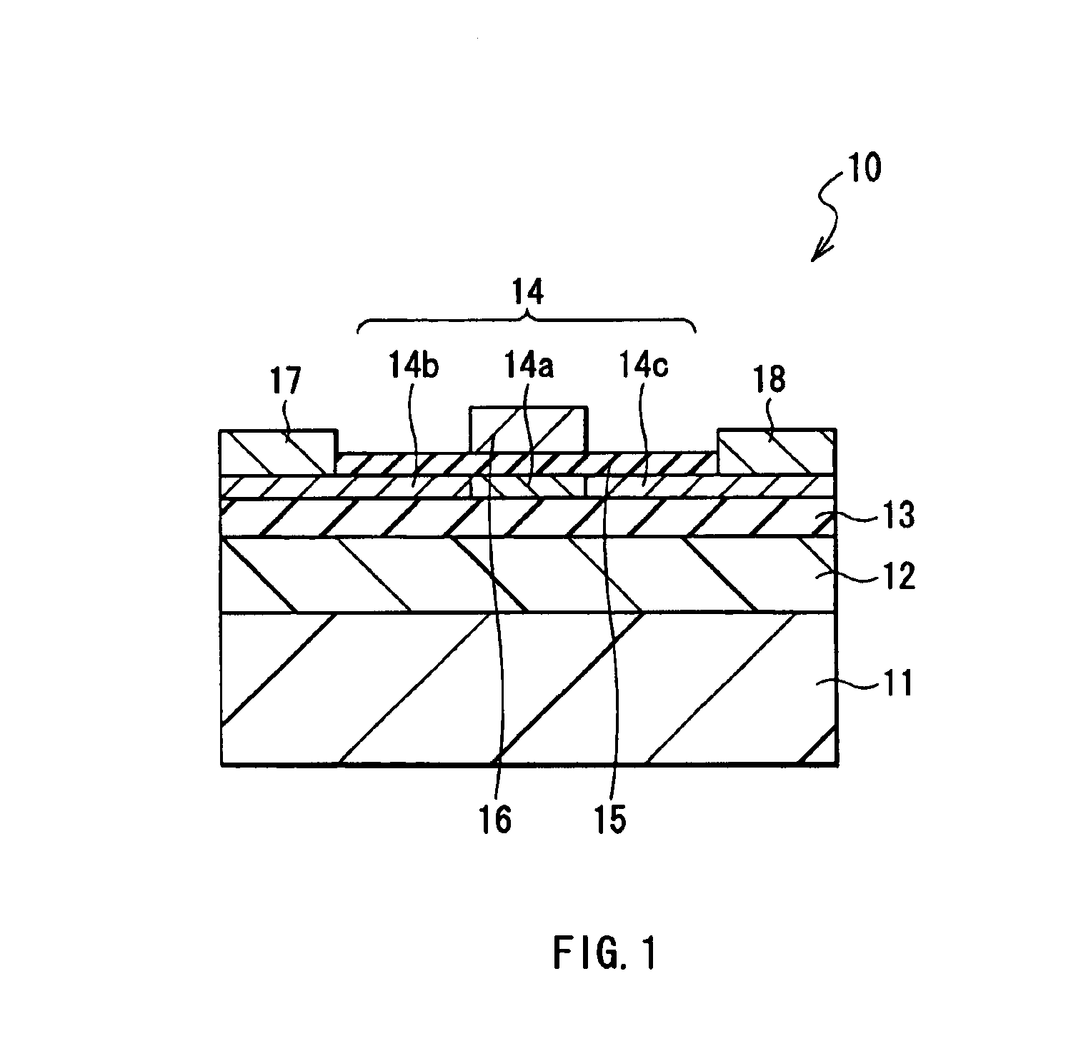
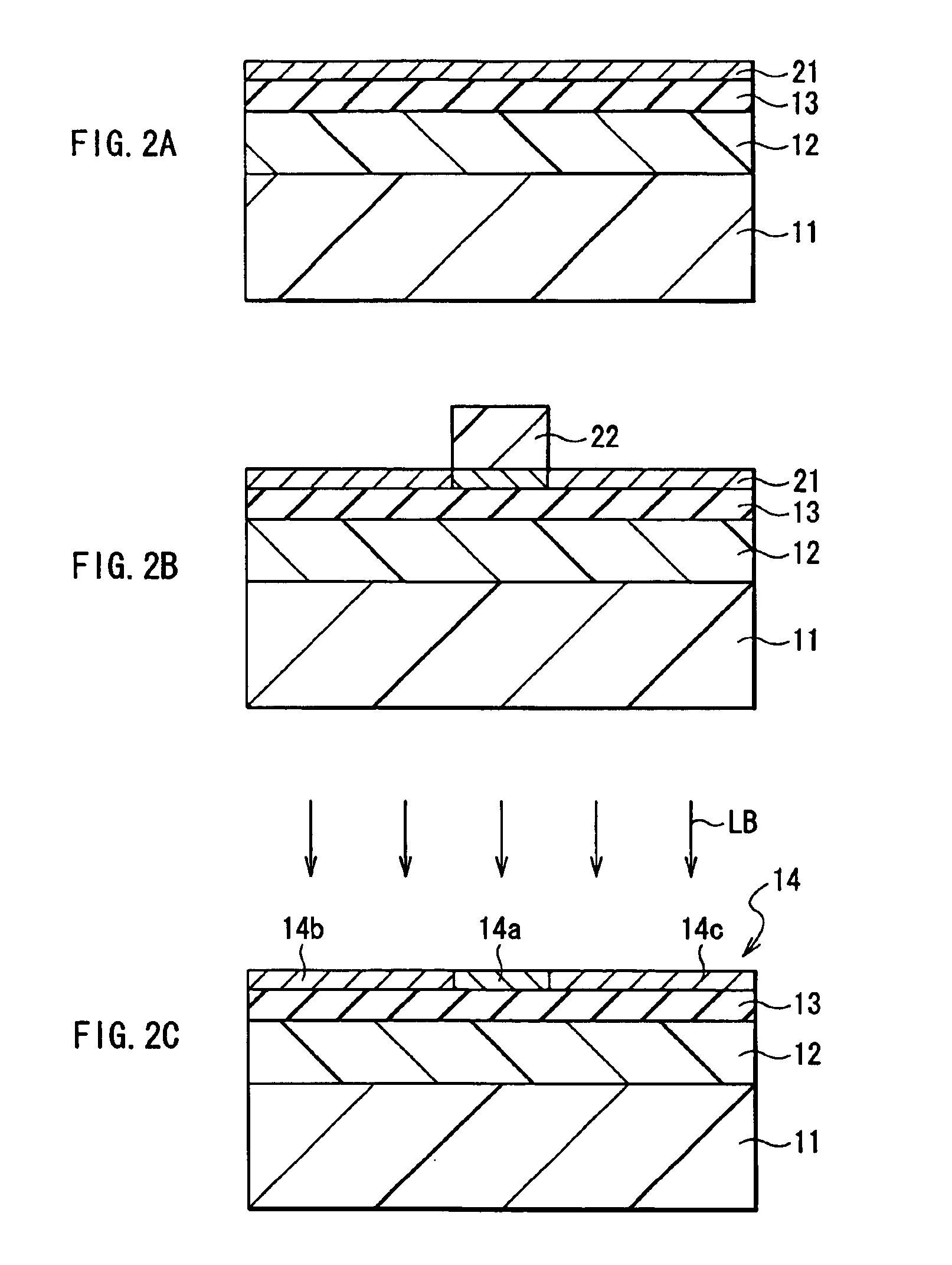
[0024]FIG. 1 shows a sectional configuration of a thin film transistor 10 according to a first embodiment of the invention. The thin film transistor 10 has, for example, an organic polymer layer 12 and an inorganic heat resistant layer 13 which are stacked in this order on a substrate 11. The thickness increases in accordance with the order of the inorganic heat resistant layer 13, the organic polymer layer 12, and the substrate 11. On the inorganic heat resistant layer 13, a channel area 14a, a source area 14b, and a drain area 14c are formed as a functional layer 14. The source area 14b and the drain area 14c are provided so as to be isolated from each other and adjacent to the channel area 14a. A gate electrode 16 is formed on the channel area 14a via an insulating film 15. A source electrode 17 is electrically connected to the source area 14b, and a drain electrode 18 is electrically connected to the drain area 14c.

[0025]The substrate 11 is made of, for example, an organic mate...

second embodiment

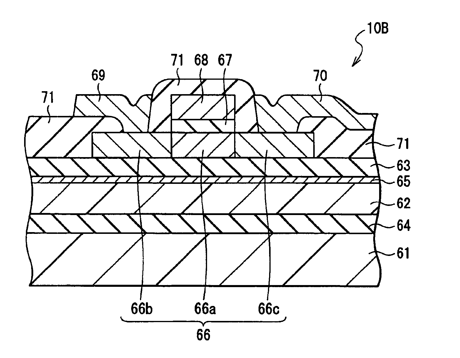
[0049]FIG. 4 shows a sectional configuration of a thin film transistor 10B according to a second embodiment of the invention. In the thin film transistor 10B, for example, between a substrate 61 and a functional layer 66, an inorganic heat resistant layer 64, an organic polymer layer 62, a metal layer 65, and an inorganic heat resistant layer 63 are stacked in order. The inorganic heat resistant layer 63 is provided on the top face of the organic polymer layer 62 in a manner similar to the first embodiment, and the inorganic heat resistant layer 64 is provided on the under face of the organic polymer layer 62. The inorganic heat resistant layers 63 and 64 are made of, for example, similar materials. The functional layer 66 has a channel area 66a, a source area 66b, and a drain area 66c. A gate electrode 68 is formed on the channel area 66a via an insulating film 67, a source electrode 69 is electrically connected to the source area 66b, and a drain electrode 70 is electrically conne...

third embodiment

[0059]FIG. 5 shows a sectional configuration of a dielectric capacitor 30 according to the second embodiment of the invention. The dielectric capacitor 30 has, in a manner similar to the thin film transistor 10 of the first embodiment, the substrate 11, organic polymer layer 12, and inorganic heat resistant layer 13. The same components are designated by the same reference numerals as those of the first embodiment and their detailed description will not be repeated.

[0060]On the inorganic heat resistant layer 13, for example, a lower electrode 31 made of indium tin oxide (ITO), a dielectric layer 32 as a functional layer, and an upper electrode 33 made of ITO are stacked in this order from a side close to the inorganic heat resistant layer 13. The dielectric layer 32 is, for example, polycrystalline and contains a ferroelectric material such as solid solution (PZT) of lead titanate (PbTiO3) and lead zirconate (PbZrO3), barium titanate (BaTiO3), or a layer structure oxide containing b...


PUM

PropertyMeasurementUnit
carrier mobilityaaaaaaaaaa
thicknessaaaaaaaaaa
thicknessaaaaaaaaaa

Abstract

The invention provides a functional device having no cracks and capable of delivering good functional characteristics and a method of manufacturing the same. A functional layer (14) is formed by crystallizing an amorphous silicon layer as a precursor layer by laser beam irradiation. A laser beam irradiation conducts heat up to a substrate (11) to cause it to try to expand; a stress to be produced by the difference in thermal expansion coefficient between the substrate (11) and the functional layer (14) is shut off by an organic polymer layer (12) lower in thermal expansion coefficient than the substrate (11), thereby causing no cracks nor separations in the functional layer (14). The organic polymer layer (12) is preferably made of an acrylic resin, an epoxy resin, or a polymer material containing these that is deformed by an optical or thermal process to undergo a three-dimensional condensation polymerization, for higher compactness and hardness. Inserting a metal layer and an inorganic heat resistant layer between the substrate (11) and the functional layer (14) will permit a more powerful laser irradiation.

Description

BACKGROUND OF THE INVENTION[0001]The present invention relates to a functional device having a functional layer, such as a thin film transistor, a dielectric capacitor, or a solar battery, and a method of manufacturing the same.[0002]Since the pn junction of a hydrogenated amorphous silicon was developed in 1976, the hydrogenated amorphous silicon has been being actively studied. The hydrogenated amorphous silicon has a structure in which a dangling bond in a network made of silicon is terminated by hydrogen or fluorine, and its film can be formed at a low temperature equal to or lower than 300° C. Consequently, the film can be formed on a cheap glass substrate. A study is being made to apply the hydrogenated amorphous silicon to a functional device such as a thin film transistor (TFT), a solar battery, or an optical sensor.[0003]However, when the hydrogenated amorphous silicon is used as it is, in the case of a TFT, only carrier mobility as low as about 0.1 to 0.5 cm2 / V·s can be ob...

Claims


Application Information

Patent Timeline
Patent Type & Authority Patents(United States)
IPC IPC(8): H01L21/336H01L29/786H01L29/66H01L21/20H01L21/02H01L21/268B32B7/02H01L21/822H01L27/04H01L31/04
CPCH01L21/2026H01L29/66757H01L29/66765H01L29/78603H01L29/78675H01L29/78678H01L21/268H01L21/02532H01L21/02686H01L29/78
Inventor MACHIDA, AKIOGOSAIN, DHARAM PALUSUI, SETSUO
Owner SONY CORP
Why Eureka
Try Eureka