Liquid crystal display device

a liquid crystal display and monolithic technology, applied in semiconductor devices, instruments, optics, etc., can solve the problems of film stress left in the sin layer, disadvantageous impeded adhesion and uniformity of the polyimide orientation film, and inability to adjust the characteristics of the transistor

Inactive Publication Date: 2003-04-29
SONY CORP
View PDF28 Cites 82 Cited by
  • Summary
  • Abstract
  • Description
  • Claims
  • Application Information

AI Technical Summary

Benefits of technology

It is another object of the invention to provide a liquid crystal display device of the type which has a TFT lower substrate and an upper substrate substantially entirely opposed to each other wherein thin film transistors on the lower substrate are covered with a passivation layer made of an oxide film thereby ensuring stable transistor characteristics.
It is a further object of the invention to provide a liquid crystal display device of the above-mentioned type wherein a passivation layer made of an oxide film and a silicon nitride layer which is selectively formed on thin film transistors and wiring layers is formed whereby the thin film transistor characteristics are prevented from degradation effectively and breakage of the wiring layers is also prevented.

Problems solved by technology

When a SiN-based insulating film is used as the protective film instead of the SiO.sub.2 -based compound within the liquid crystal cell, the adhesiveness and uniformity of the polyimide orientation film are disadvantageously impeded.
As a result, the orientation of the liquid crystal is in turn impeded.
In addition, when the SiN-based protective layer is formed on the upper portion of the TFT transistor, the film stress left in the SiN layer will undesirably change the transistor characteristics, e.g. the V.sub.TH characteristic is shifted.
Thus, the problem involved in the SiN insulating film is still left.
At the grain boundaries, trapping levels are so high that carriers are trapped.
Accordingly, the mobility of the carriers in the polycrystals becomes low, making it difficult to obtain a satisfactory on-current.
When the silicon nitride film which has been hydrogenated is left as it is as a passivation layer, there is produced a disadvantage in that the silicon nitride film has a high residual stress, bringing about a significant variation in electric characteristics and particularly a threshold voltage of the thin film transistor.
Moreover, when a liquid crystal orienting film such as polyimide is directly formed on the silicon nitride protective film, a disadvantage is involved in that the adhesion between the orienting film and the silicon nitride protective film is not good, resulting in poor uniformity of the orienting film.
In addition, when a pair of the substrates are bonded to assemble a liquid crystal cell while leaving the silicon nitride protective film, there is not obtained a satisfactory adhesion strength.

Method used


Image

  • Liquid crystal display device
  • Liquid crystal display device
  • Liquid crystal display device

Examples


first embodiment

In the first embodiment, the silicon nitride film is completely removed in the fabrication process. The complete removal of the silicon nitride film is advantageous as stated hereinabove. However, there may be some possibility that the hydrogen atoms diffused in the polysilicon thin film may be released owing to the stress which has been imparted after the hydrogenation treatment. This eventually leads, more or less, to degradation of electric characteristics of the transistors. The stresses may include ashing of the photoresist, plasma damages produced during the formation of the contact hole and thermal damages generated during annealing of the picture element electrode. In addition, breakage of metallic wirings may occur due to the use of etchants during the fabrication process.

In order to avoid these defects and further improve the reliability of the liquid crystal display device, there is provided a second embodiment of the invention wherein the silicon nitride is left selectiv...

second embodiment

the invention is particularly described with reference to FIGS. 22 to 25.

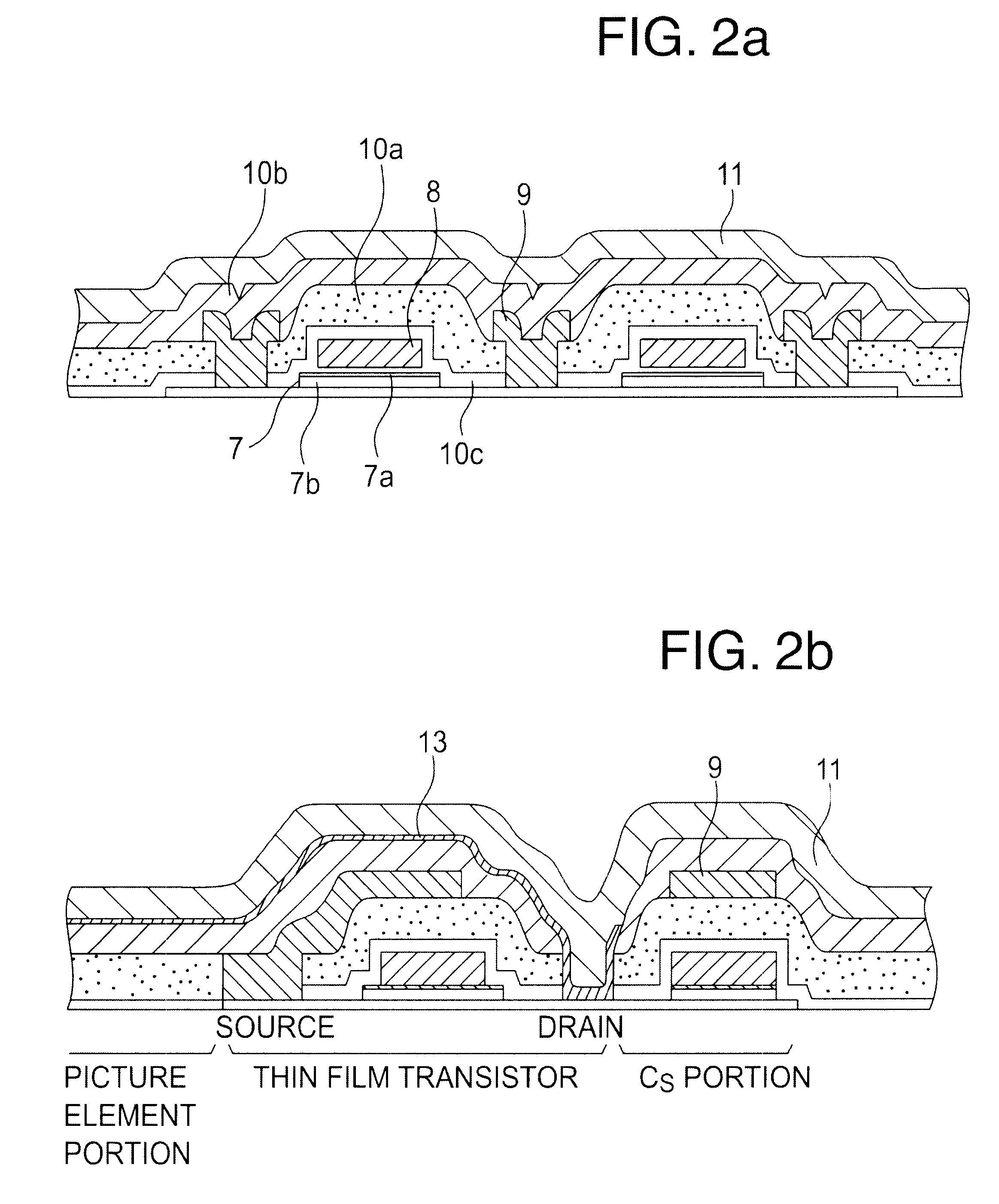
FIGS. 22a and 22b, respectively, show a peripheral circuit region and a picture element region similar to FIGS. 2a and 2b illustrating the first embodiment.

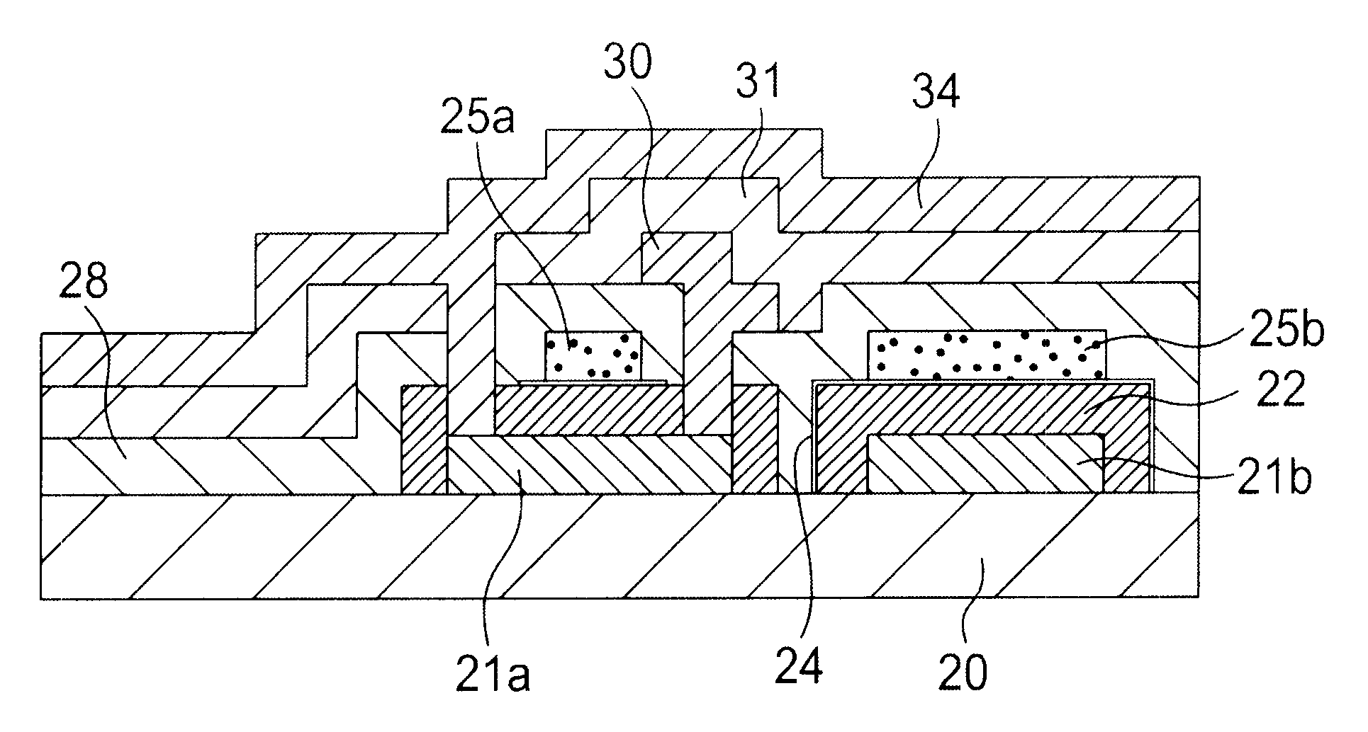
As shown in FIG. 22a, there is shown a lower substrate 101 which includes a patterned first polysilicon film 2, with which a thin film transistor is made. In this instance, the transistor has a CMOS structure contained in a peripheral circuit such as, for example, a horizontal drive circuit or a vertical drive circuit. The CMOS structure is comprised of a N-channel thin film transistor 103 and a P-channel thin film transistor 104. The respective transistors include a gate insulating film 105 with a three-layer structure and a gate electrode 106 formed on the gate insulating film 105. The gate electrode 106 is made of a patterned second polysilicon film. The gate insulating film 105 has a three-layer structure, for example, of SiO.sub.2 / SiN / SiO.sub.2. These ...


PUM

PropertyMeasurementUnit
temperatureaaaaaaaaaa
thicknessaaaaaaaaaa

Abstract

A liquid crystal display device of the monolithic type which comprises a first substrate, a plurality of display elements arranged in a matrix on the first substrate to define a display area of the liquid crystal display device, each of the display elements comprising a picture element or pixel electrode and a switching or pixel transistor associated with the picture element or pixel electrode, a driving circuit formed on the first substrate and connected to the display area. The driving circuit includes a horizontal driver and a vertical driver. The device further includes a second substrate substantially entirely opposed to the first substrate, and a liquid crystal layer disposed between the first and second substrates. A passivation layer is provided to cover the display area or pixel transistors and driving circuit.

Description

1. Field of the InventionThis invention relates to a monolithic liquid crystal display device of the active matrix type which has a thin film transistor drive circuit in a liquid crystal cell and more particularly, to a passivation structure of a thin film transistor in the liquid crystal display device.2. Description of the Prior ArtA known liquid crystal display device is first described. FIG. 21 schematically shows a known liquid crystal display device which includes a horizontal drive 4 and a vertical driver 5, each formed with a thin film transistor (TFT), outside a liquid cell unit U. The liquid cell unit U alone is so arranged that a liquid crystal layer (not shown) is sealed in a spacer 16 sandwiched between an upper substrate 14 and a lower substrate 15 which are opposed to each other. In other words, the lower substrate 15 serving as a substrate for the TFT's is made larger in size than the upper substrate 14 to define a marginal substrate portion on which the peripheral d...

Claims


Application Information

Patent Timeline
Patent Type & Authority Patents(United States)
IPC IPC(8): G02F1/13G02F1/1362G02F1/1345G02F1/136G02F1/1368
CPCG02F1/13454G02F1/133
Inventor INO, MASUMITSU
Owner SONY CORP
Why Eureka
Try Eureka