Non-volatile memory devices including variable resistance material

a variable resistance material and memory device technology, applied in semiconductor devices, digital storage, instruments, etc., can solve the problems of less integration density and/or operating speed of non-volatile memory devices, the difficulty of increasing the integration of these types of related art prams, and the loss of stored data of drams, etc., to achieve stable electrical characteristics, improve integration, and simplify the effect of structur

Active Publication Date: 2007-11-01
SAMSUNG ELECTRONICS CO LTD
View PDF10 Cites 57 Cited by
  • Summary
  • Abstract
  • Description
  • Claims
  • Application Information

AI Technical Summary

Benefits of technology

[0010]Example embodiments provide non-volatile memory devices having a simplified and / or improved structure, which may be more suitable for higher integration and / or more stable electrical characteristics.

Problems solved by technology

However, DRAMs are volatile in that when the power supply is shut down, DRAMs lose stored data.
Unlike volatile memory devices, non-volatile memory retains data when power is shut-off; however, related art non-volatile memory devices have lower integration density and / or operating speed than volatile memories, such as, DRAMs.
However, increasing integration of these types of related art PRAMs may be more difficult to fabricate due to their structural characteristics.
As shown, a process of forming a related art electrode (e.g., upper electrode 16) may also be relatively difficult if the electrode has an etch slope of about 40 degrees.
Furthermore, when a precious metal such as Pt is used to form the electrode, fabrication costs in the production of memory devices increase.

Method used


Image

  • Non-volatile memory devices including variable resistance material
  • Non-volatile memory devices including variable resistance material
  • Non-volatile memory devices including variable resistance material

Examples


Embodiment Construction

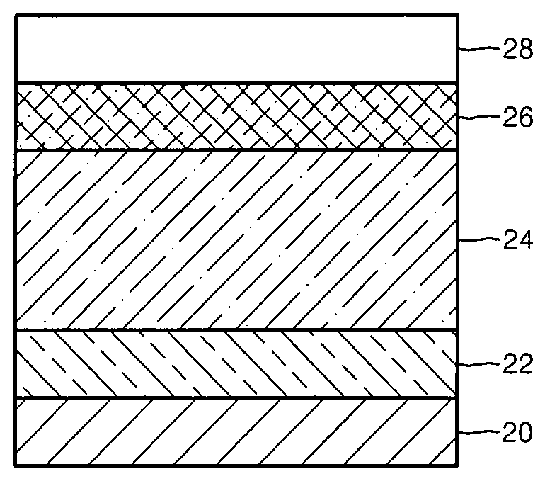
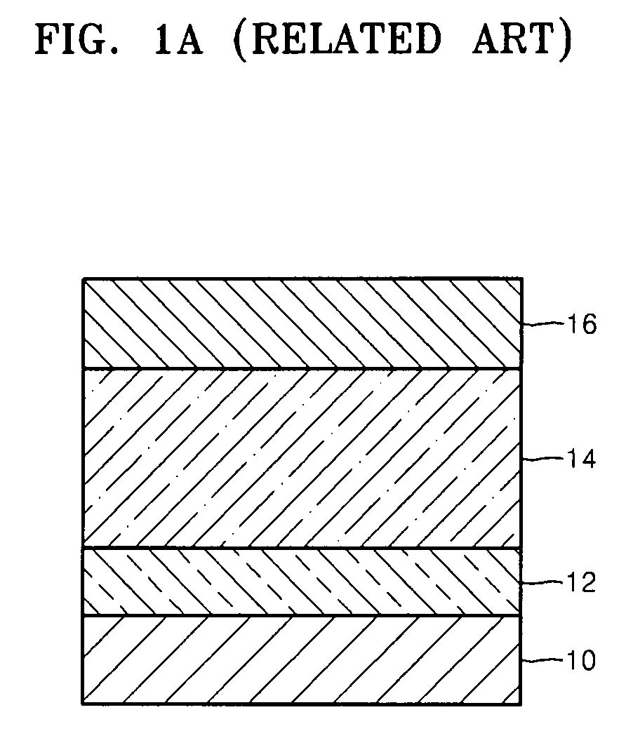
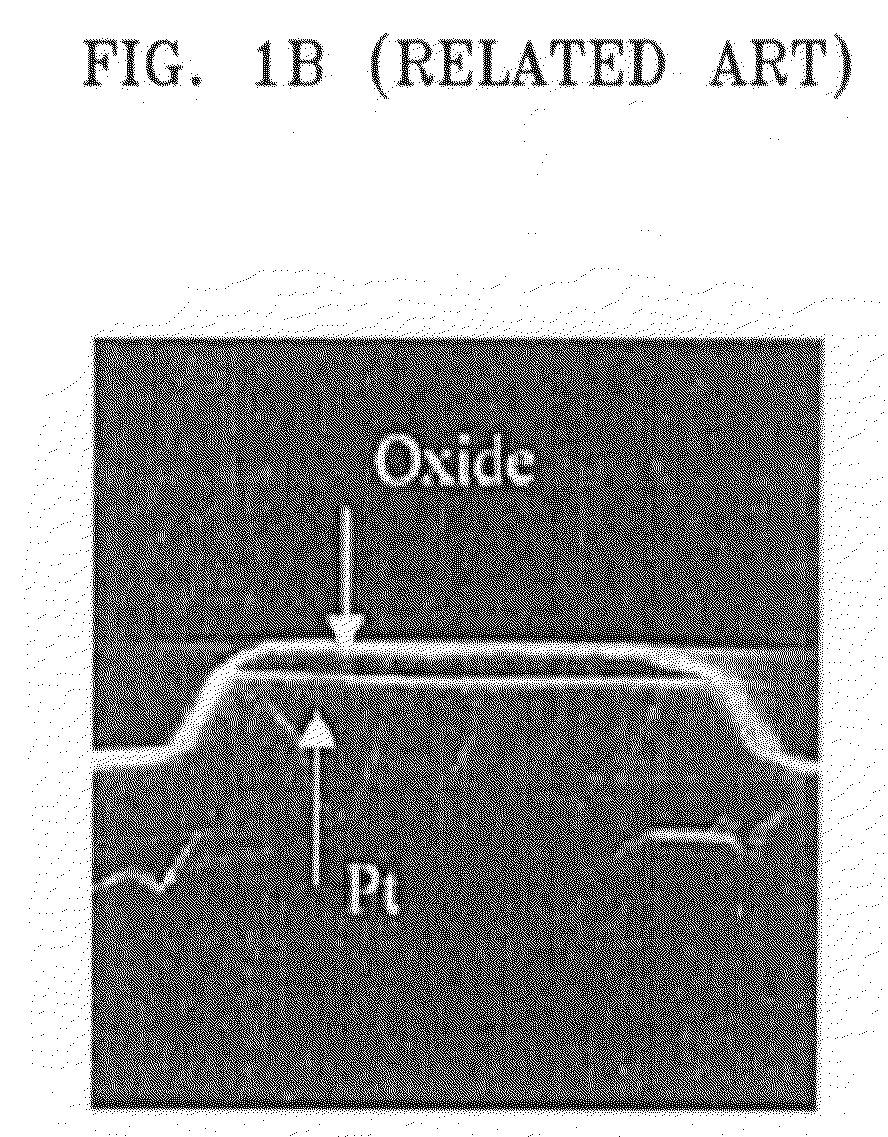
[0027]Various example embodiments will now be described more fully with reference to the accompanying drawings in which some example embodiments are shown. In the drawings, the thicknesses of layers and regions are exaggerated for clarity.

[0028]Detailed illustrative example embodiments are disclosed herein. However, specific structural and functional details disclosed herein are merely representative for purposes of describing example embodiments. This invention may, however, may be embodied in many alternate forms and should not be construed as limited to only the example embodiments set forth herein.

[0029]Accordingly, while example embodiments are capable of various modifications and alternative forms, embodiments thereof are shown by way of example in the drawings and will herein be described in detail. It should be understood, however, that there is no intent to limit example embodiments to the particular forms disclosed, but on the contrary, example embodiments are to cover all...


PUM

PropertyMeasurementUnit
voltageaaaaaaaaaa
variable resistance characteristicsaaaaaaaaaa
integration densityaaaaaaaaaa

Abstract

A non-volatile memory device comprises a first oxide layer, a second oxide layer and a buffer layer formed on a lower electrode. An upper electrode is formed on the buffer layer. In one example, the lower electrode is composed of at least one of Pt, Ru, Ir, IrOx and an alloy thereof, the second oxide layer is a transition metal oxide, the buffer layer is composed of a p-type oxide and the upper electrode is composed of a material selected from Ni, Co, Cr, W, Cu or an alloy thereof.

Description

PRIORITY STATEMENT[0001]This non-provisional U.S. patent application claims priority under 35 U.S.C. § 119 to Korean Patent Application No. 10-2006-0038844, filed on Apr. 28, 2006, in the Korean Intellectual Property Office (KIPO), the entire contents of which is incorporated herein by reference.BACKGROUNDDescription of the Related Art[0002]Related art semiconductor memory devices include a relatively large number of memory cells connected by circuits. In a dynamic random access memory (DRAM), for example, a unit memory cell may comprise one switch and one capacitor. A DRAM may have a relatively high integration density and operating speed. However, DRAMs are volatile in that when the power supply is shut down, DRAMs lose stored data.[0003]In related art non-volatile memory devices, such as flash memory devices, stored data is maintained even when the power is cut off. Unlike volatile memory devices, non-volatile memory retains data when power is shut-off; however, related art non-v...

Claims


Application Information

Patent Timeline
Patent Type & Authority Applications(United States)
IPC IPC(8): H01L29/788
CPCG11C11/5685G11C13/0007G11C2213/15G11C2213/32G11C2213/34G11C2213/52H01L45/146H01L29/24H01L29/8615H01L45/12H01L45/04H01L45/1233H01L27/101H10N70/801H10N70/20H10N70/826H10N70/8833
Inventor CHO, CHOONG-RAELEE, EUN-HONGBOURIM, EL MOSTAFAMOON, CHANG-WOOK
Owner SAMSUNG ELECTRONICS CO LTD
Why Eureka
Try Eureka