Nonvolatile memory element, nonvolatile memory apparatus, nonvolatile semiconductor apparatus, and method of manufacturing nonvolatile memory element

a nonvolatile memory and semiconductor technology, applied in semiconductor devices, digital storage, instruments, etc., can solve the problem of limiting the miniaturization of an existing flash memory using a floating gate, and achieve the effect of stable rewrite characteristic and high affinity

Active Publication Date: 2009-09-10
PANASONIC SEMICON SOLUTIONS CO LTD
View PDF8 Cites 55 Cited by
  • Summary
  • Abstract
  • Description
  • Claims
  • Application Information

AI Technical Summary

Benefits of technology

[0034]In accordance with the present invention, a nonvolatile memory element which is capable of high-speed operation, has a reversibly stable rewrite characteristic and a desired retention characteristic of a resistance value, and has high affinity with a semiconductor manufacturing process, and a manufacturing method thereof, and a nonvolatile semiconductor apparatus or the like including the nonvolatile memory element.

Problems solved by technology

In response to such demands, it is said that there is a limitation on miniaturization of an existing flash memory using a floating gate.

Method used


Image

  • Nonvolatile memory element, nonvolatile memory apparatus, nonvolatile semiconductor apparatus, and method of manufacturing nonvolatile memory element
  • Nonvolatile memory element, nonvolatile memory apparatus, nonvolatile semiconductor apparatus, and method of manufacturing nonvolatile memory element
  • Nonvolatile memory element, nonvolatile memory apparatus, nonvolatile semiconductor apparatus, and method of manufacturing nonvolatile memory element

Examples


embodiment 1

Configuration of Nonvolatile Memory Element

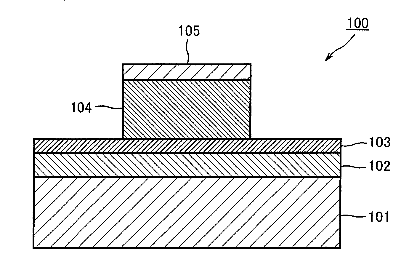
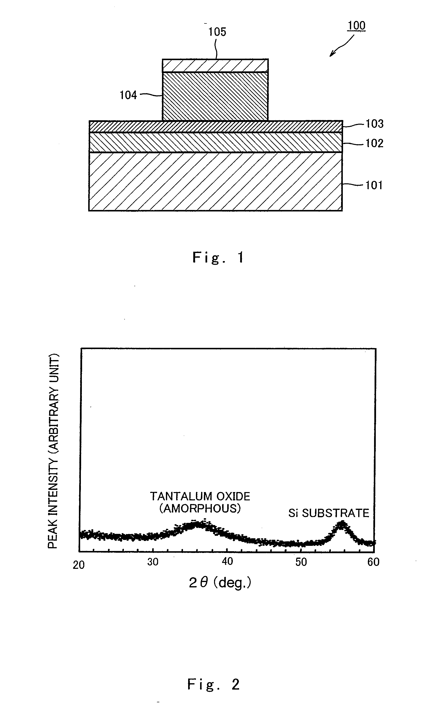
[0127]FIG. 1 is a cross-sectional view showing an example of a configuration of the nonvolatile memory element according to Embodiment 1 of the present invention.

[0128]As shown in FIG. 1, the nonvolatile memory element 100 includes a substrate 101, an oxide layer 102 formed on the substrate 101, a first electrode layer 103 formed on the oxide layer 102, a second electrode 105, and a resistance variable layer 104 sandwiched between the first electrode layer 103 and the second electrode layer 105.

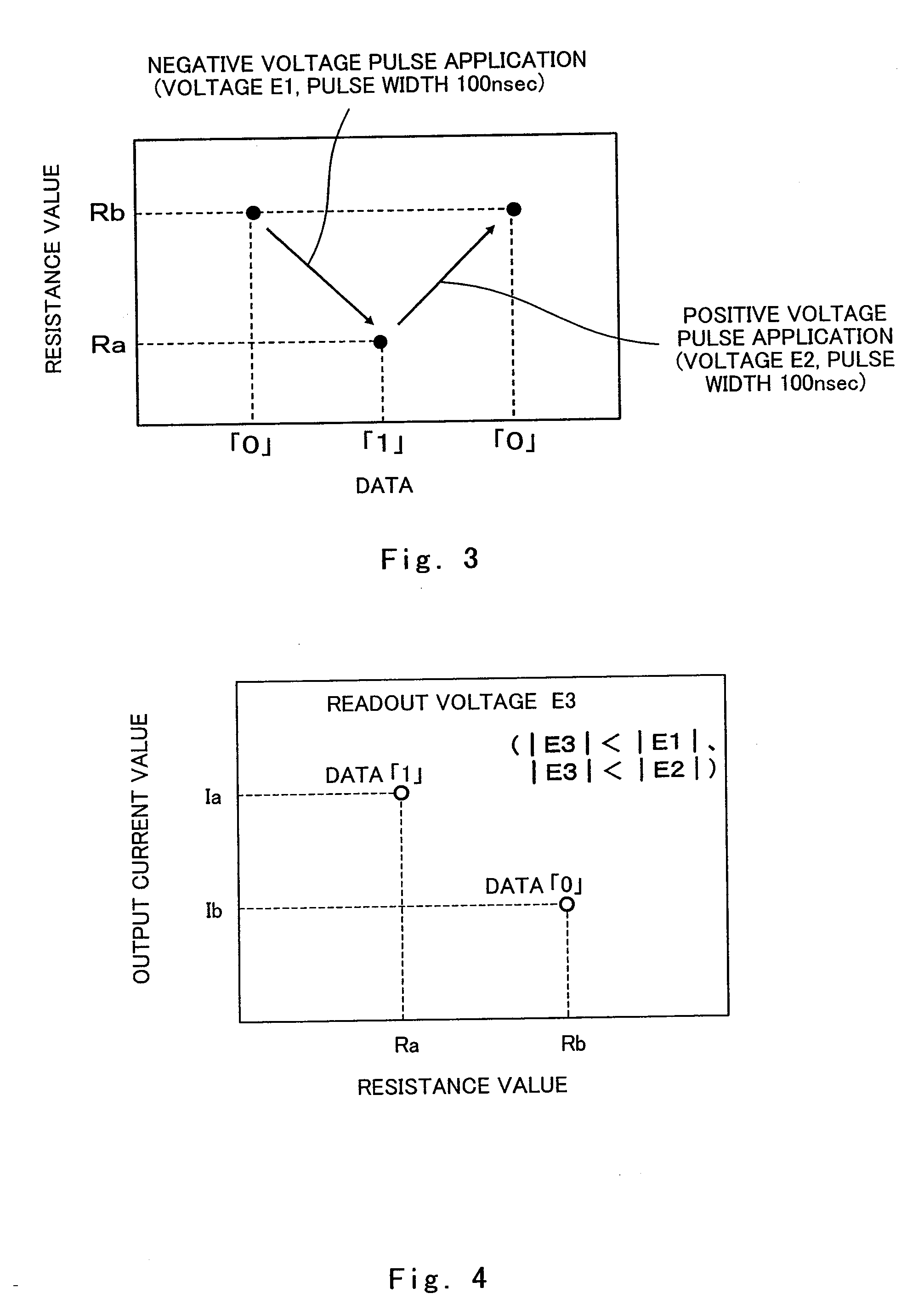
[0129]When the nonvolatile memory element 100 is driven, a voltage (electric signal) meeting a predetermined condition is applied between the first electrode layer 103 and the second electrode 105 from an external electric power supply. The resistance value of the resistance variable layer 104 of the nonvolatile memory element 100 increases or decreases according to the direction (the polarity of voltage) in which the voltage is applied. For example,...

embodiment 2

[0187]The above described nonvolatile memory element according to Embodiment 1 is applicable to nonvolatile semiconductor apparatuses having various configurations. A semiconductor apparatus according to Embodiment 2 is a nonvolatile memory apparatus which includes the nonvolatile memory element according to Embodiment 1 and is a cross-point type memory apparatus in which an active layer intervenes at an intersection (three-dimensional cross-point) between a word line and a bit line.

Configuration of Semiconductor Apparatus According to Embodiment 2

[0188]FIG. 20 is a block diagram showing a configuration of a nonvolatile memory apparatus according to Embodiment 2 of the present invention. FIG. 21 is a perspective view showing a configuration (configuration corresponding to 4 bits) in A part of FIG. 20.

[0189]As shown in FIG. 20, a nonvolatile memory apparatus 200 according to this embodiment includes a memory main body 201 on a semiconductor substrate. The memory main body 202 include...

embodiment 3

[0233]A nonvolatile memory apparatus according to Embodiment 3 is a nonvolatile memory apparatus which includes the nonvolatile memory element according to Embodiment 1, and is of a one transistor / one nonvolatile memory portion type.

Configuration of Nonvolatile Memory Apparatus According to Embodiment 3

[0234]FIG. 26 is a block diagram showing a configuration of a nonvolatile memory apparatus according to Embodiment 3 of the present invention. FIG. 27 is a cross-sectional view showing a configuration (configuration corresponding to 2 bits) in C part of FIG. 26.

[0235]As shown in FIG. 26, a nonvolatile memory apparatus 300 according to this embodiment includes a memory main body 301 on a semiconductor substrate. The memory main body 301 includes a memory array 302, a row selection circuit / driver 303, a column selection circuit 304, a write circuit 305 for writing data, a sense amplifier 306 which detects an amount of a current flowing in a selected bit line and determines the data as “...


PUM


Abstract

A nonvolatile memory element of the present invention comprises a first electrode (103), a second electrode (105), and a resistance variable layer (104) disposed between the first electrode (103) and the second electrode (104), a resistance value of the resistance variable layer varying reversibly according to an electric signal applied between the electrodes (103),(105), and the resistance variable layer (104) comprises at least a tantalum oxide, and is configured to satisfy 0<x<2.5 when the tantalum oxide is represented by TaOx.

Description

TECHNICAL FIELD[0001]The present invention relates to a nonvolatile memory element, a nonvolatile memory apparatus, a nonvolatile semiconductor apparatus, and a method of manufacturing a nonvolatile memory element. More particularly, the present invention relates to a resistance variable nonvolatile memory element, a resistance variable nonvolatile memory apparatus, and a resistance variable nonvolatile semiconductor apparatus, whose resistance values vary according to electric signals applied.BACKGROUND ART[0002]With recent advancement of digital technologies, higher functionality of electronic hardware such as portable information devices and home information appliances have been provided. For this reason, demands for an increase in a capacity of a nonvolatile memory element, a reduction in writing electric power in the memory element, a reduction in write / readout time in the memory element, and longer life of the memory element have been increasing.[0003]In response to such deman...

Claims


Application Information

Patent Timeline
Patent Type & Authority Applications(United States)
IPC IPC(8): H01L47/00H01L21/00
CPCG11C13/0007G11C2213/32G11C2213/34G11C2213/71G11C2213/72G11C2213/79H01L45/1233H01L27/2418H01L27/2436H01L27/2481H01L45/08H01L45/146H01L45/1625H01L27/101H10B63/22H10B63/30H10B63/84H10N70/24H10N70/826H10N70/8833H10N70/026H10N70/231
Inventor FUJII, SATORUTAKAGI, TAKESHIMURAOKA, SHUNSAKUOSANO, KOICHISHIMAKAWA, KAZUHIKO
Owner PANASONIC SEMICON SOLUTIONS CO LTD
Why Eureka
Try Eureka