Semiconductor device and method for manufacturing thereof

a semiconductor device and semiconductor technology, applied in the field of semiconductor devices, can solve the problems of reducing the reliability of a semiconductor device, affecting the performance of the device, and the likely effect of short channel effect, and achieve the effects of suppressing defects, high reliability, and stable electric characteristics

Active Publication Date: 2012-10-25
SEMICON ENERGY LAB CO LTD
View PDF4 Cites 59 Cited by
  • Summary
  • Abstract
  • Description
  • Claims
  • Application Information

AI Technical Summary

Benefits of technology

[0028]According to one embodiment of the disclosed invention, a semiconductor device which is miniaturized and in which defects are suppressed can be provided. Further, according to one embodiment of the disclosed invention, a semiconductor device having stable electric characteristics and high reliability can be provided.
[0029]Further, according to one embodiment of the disclosed invention, the size of a transistor can be sufficiently reduced. When the size of the transistor is sufficiently reduced, the area of a semiconductor dev...

Problems solved by technology

In the case where a transistor is miniaturized, there is a problem caused by a short channel effect.
The short channel effect is likely to occur in a transistor including an oxide semiconductor particularly because such a transistor is difficult to control threshold voltage by doping, unlike a transistor including silico...

Method used


Image

  • Semiconductor device and method for manufacturing thereof
  • Semiconductor device and method for manufacturing thereof
  • Semiconductor device and method for manufacturing thereof

Examples


embodiment 1

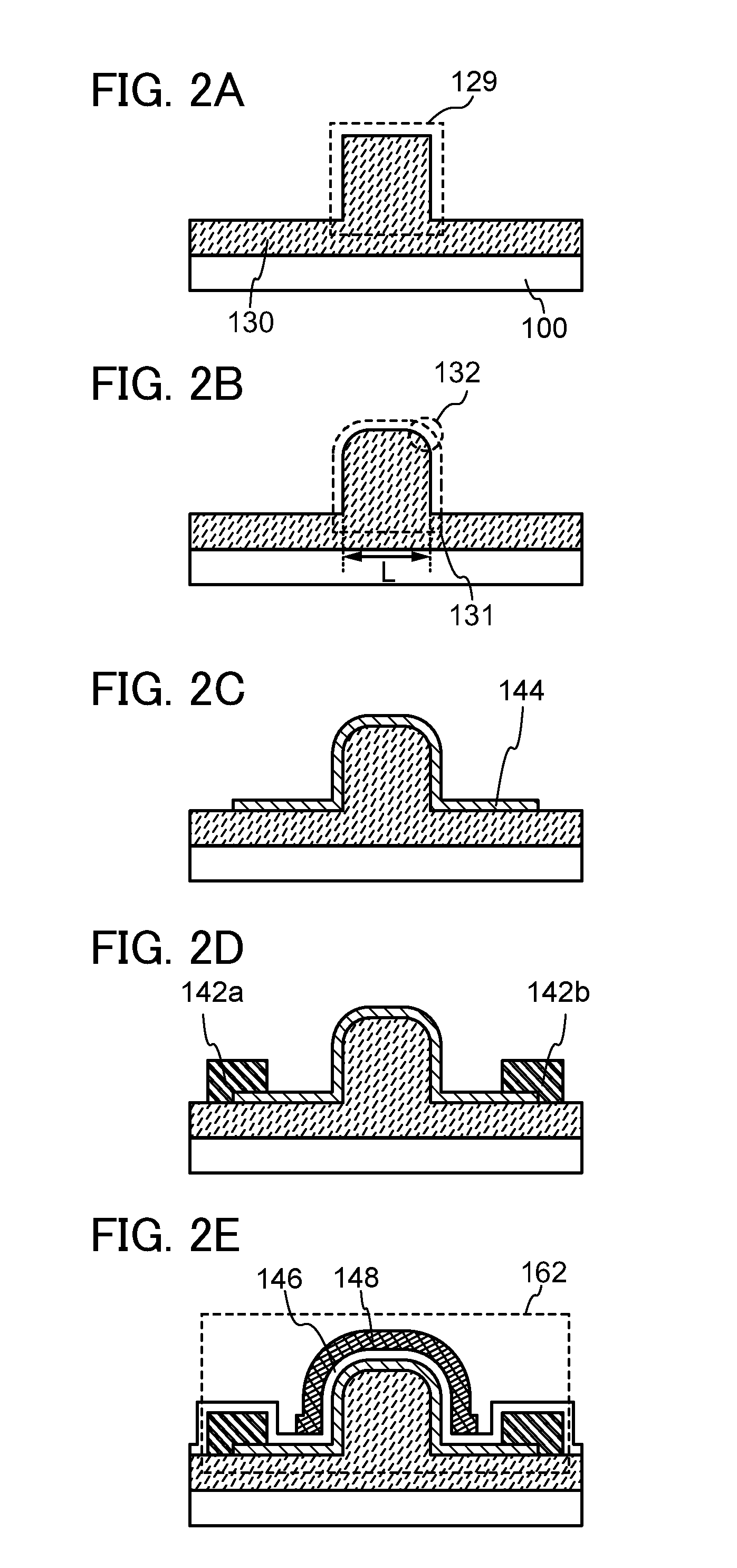
[0046]In this embodiment, as one embodiment of the present invention, a semiconductor device including an oxide semiconductor and a method for manufacturing the semiconductor device will be described with reference to FIGS. 1A and 1B, FIGS. 2A to 2E, FIGS. 3A to 3C, and FIGS. 4A to 4C.

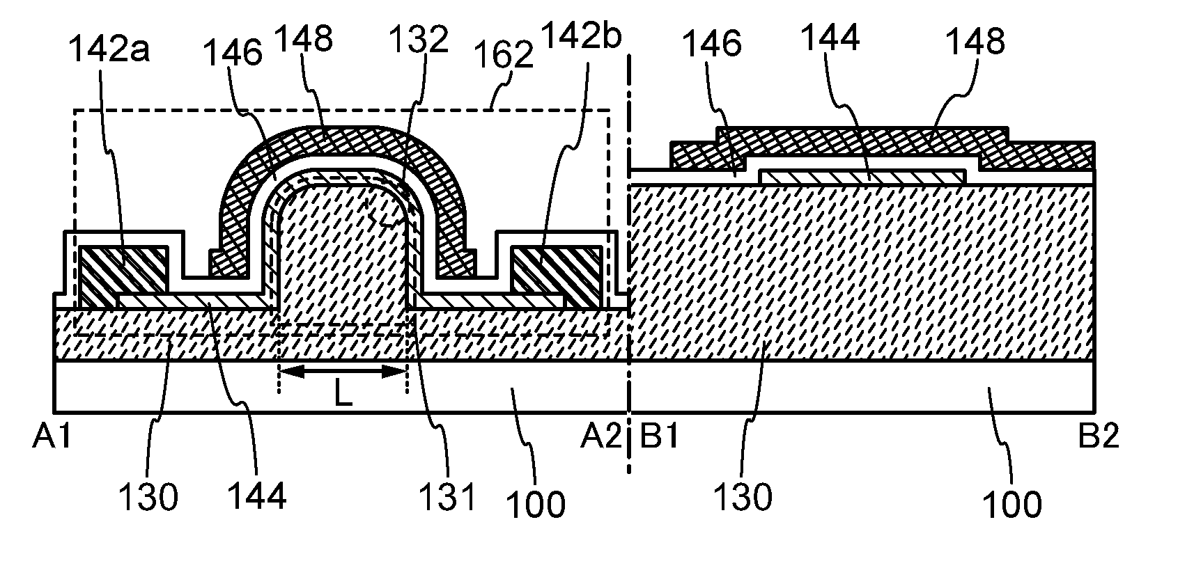
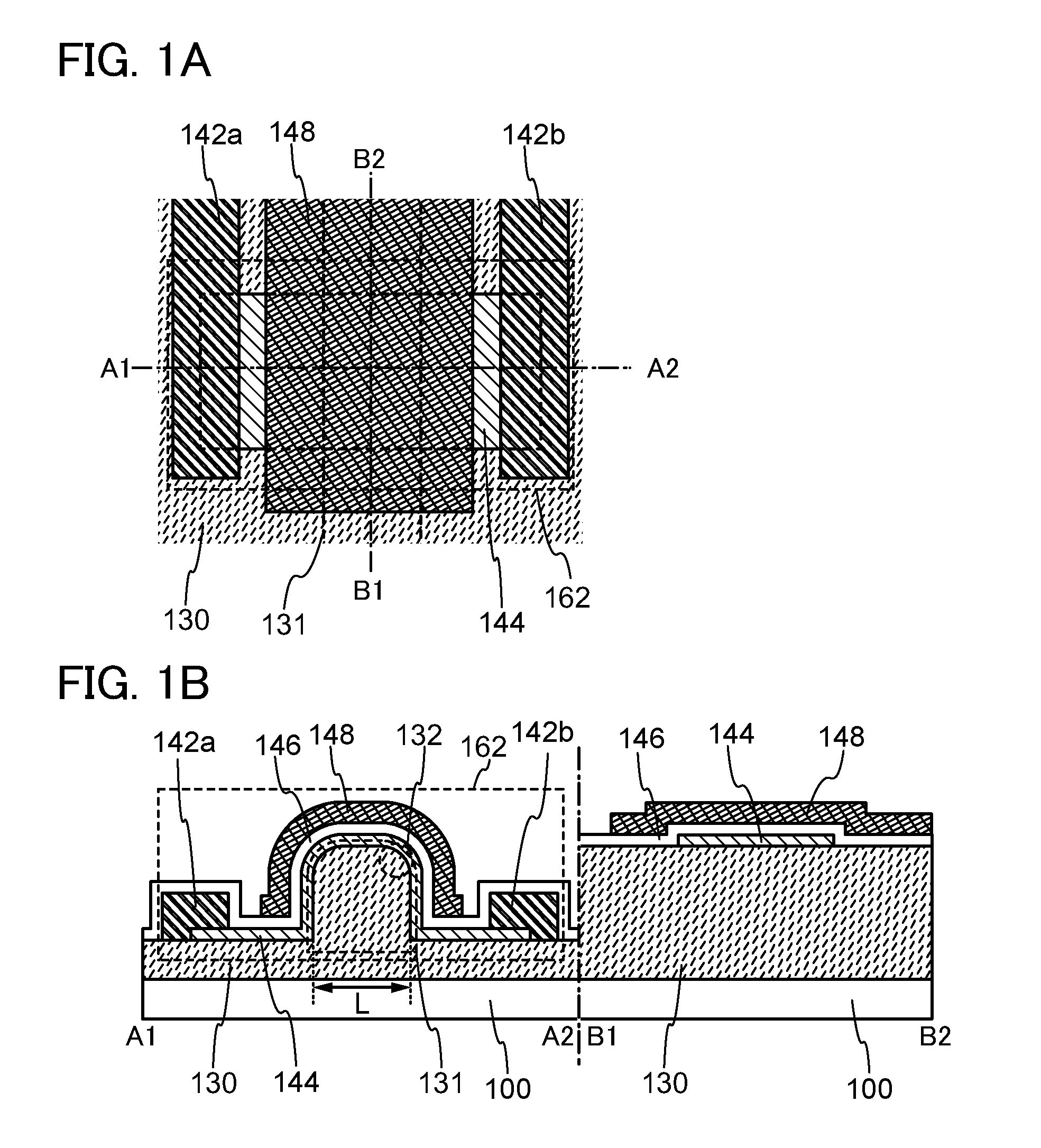
[0047]FIGS. 1A and 1B are a plan view and a cross-sectional view each illustrate a transistor 162 as an example of a semiconductor device according to one embodiment of the present invention. Here, FIG. 1B corresponds to cross sections along a line A1-A2 and a line B1-B2 in FIG. 1A.

[0048]The transistor 162 illustrated in FIGS. 1A and 1B includes an insulating layer 130 which is formed over a substrate 100 and provided with a projecting structural body 131 on its surface, an oxide semiconductor layer 144 provided in contact with at least part of a top surface and side surface of the projecting structural body 131, a gate insulating layer 146 provided over the oxide semiconductor layer 144, a gate electr...

embodiment 2

[0135]In this embodiment, as one embodiment of the present invention, a method for manufacturing a semiconductor device including an oxide semiconductor, which is different from that in the above embodiment will be described with reference to FIGS. 5A to 5E.

[0136]A structure of a transistor 262 illustrated in FIG. 5E is similar to that of the transistor 162 illustrated in FIG. 1B. The transistor 262 includes an insulating layer 230 formed over a substrate 200 and provided with a projecting structural body 231 on its surface, an oxide semiconductor layer 244 provided in contact with at least part of a top surface and side surface of the projecting structural body 231, a gate insulating layer 246 provided over the oxide semiconductor layer 244, a gate electrode 248 provided over the gate insulating layer 246 so as to cover at least part of the top surface and side surface of the projecting structural body 231, and a source electrode 242a and a drain electrode 242b which are electrical...

embodiment 3

[0173]In this embodiment, an example of a semiconductor device which includes the transistor 162 described in any of the above Embodiments, which can hold stored data even when not powered, and which has an unlimited number of write cycles will be described with reference to drawings. Needless to say, the transistor 262 described in the above Embodiments may be used instead of the transistor 162.

[0174]Since the off-state current of the transistor 162 is small, stored data can be held for a long time owing to such a transistor. In other words, it is possible to obtain a semiconductor device which does not require refresh operation or has an extremely low frequency of the refresh operation, which leads to a sufficient reduction in power consumption.

[0175]FIGS. 6A to 6C illustrate an example of a structure of the semiconductor device. FIG. 6A is a cross-sectional view of the semiconductor device, FIG. 6B is a plan view of the semiconductor device, and FIG. 6C is a circuit diagram of th...


PUM


Abstract

An insulating layer is provided with a projecting structural body, and a channel formation region of an oxide semiconductor layer is provided in contact with the projecting structural body, whereby the channel formation region is extended in a three dimensional direction (a direction perpendicular to a substrate). Thus, it is possible to miniaturize a transistor and to extend an effective channel length of the transistor. Further, an upper end corner portion of the projecting structural body, where a top surface and a side surface of the projecting structural body intersect with each other, is curved, and the oxide semiconductor layer is formed to include a crystal having a c-axis perpendicular to the curved surface.

Description

BACKGROUND OF THE INVENTION[0001]1. Field of the Invention[0002]The invention disclosed in this specification relates to a semiconductor device and a method for manufacturing the semiconductor device utilizing a semiconductor element.[0003]2. Description of the Related Art[0004]Attention has been focused on a technique of using a semiconductor thin film formed over a substrate having an insulating surface to form a transistor. The transistor is applied to a wide range of electronic devices such as an integrated circuit (IC) or an image display device (display device). Further, a technique of using a wide band gap semiconductor such as an oxide semiconductor for a semiconductor thin film that can be used for a transistor has been attracting attention.[0005]For example, Patent Document 1 shows that an oxide semiconductor including an In—Ga—Zn—O-based oxide can be used for a channel formation region of a thin film transistor.REFERENCE[0006][Patent Document 1] Japanese Published Patent ...

Claims


Application Information

Patent Timeline
IPC IPC(8): H01L29/24H01L21/34
CPCH01L21/02554H01L21/02565H01L21/02667H01L27/0688H01L29/66969H01L29/7869H01L29/78696H01L29/42384H01L29/78603H01L27/1225H01L29/04H01L29/1037H01L29/78642
Inventor ISOBE, ATSUOSASAKI, TOSHINARISASAGAWA, SHINYAISHIZUKA, AKIHIRO
Owner SEMICON ENERGY LAB CO LTD
Why Eureka
Try Eureka