

Method of producing silicon carbide single crystal
- Summary
- Abstract
- Description
- Claims
- Application Information
AI Technical Summary
Benefits of technology
Problems solved by technology
Method used
Image

Examples
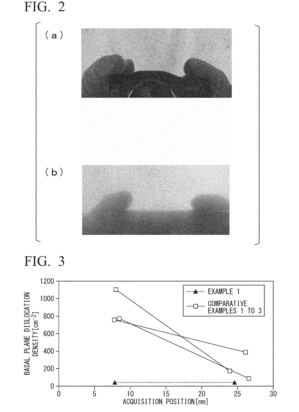
example 1
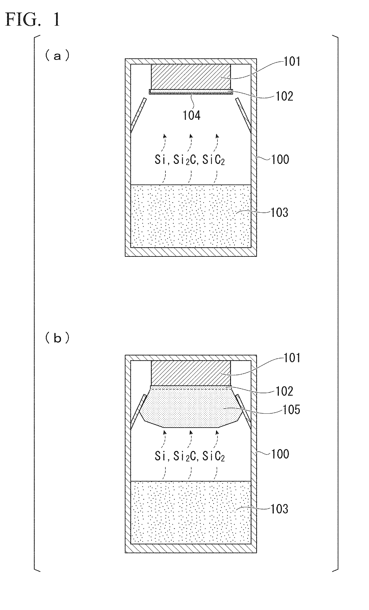
[0043]In the production method of the above embodiment, an ingot of silicon carbide single crystal was produced by carrying out from the preliminary heating to the main heating step. The pressure inside the crucible was set to 140 Torr in the all of the steps.
[0044]The preliminary heating step was performed by an induction heating system using a coil. A heating rate in the preliminary heating step was set to 420° C. / min and an interior of the crucible was heated at 2110° C. for 60 minutes.
[0045]The cooling step was performed by flowing an argon gas and a nitrogen gas (refrigerant gases) into the crucible. The cooling rate in the cooling step was 110° C. / min.
[0046]In the main heating step, a silicon carbide raw material and a crucible member were newly provided, and the induction heating method using a coil was carried out similarly to the preliminary heating step. The heating rate in the main heating step was 420° C. / min and the heating time except for the temperature rising time wa...
PUM
 Abstract
Description
Claims
Application Information