Semiconductor structure combination for epitaxy of semiconductor optoelectronic device

a semiconductor optoelectronic and semiconductor technology, applied in the field of semiconductor structure combination, can solve the problems of directly affecting the optoelectronic performance lowering the internal quantum efficiency and light-extraction efficiency of the semiconductor light-emitting device, etc., and achieve the effect of enhancing the optoelectronic performance and reducing the inner defect density of the semiconductor structure combination according to the invention

Active Publication Date: 2009-01-01
EPISTAR CORP
View PDF5 Cites 3 Cited by
  • Summary
  • Abstract
  • Description
  • Claims
  • Application Information

AI Technical Summary

Benefits of technology

[0020]Compared to the prior art, the density of inner defects of the semiconductor structure combination according to the invention can be decreased, and the semiconductor structure combination can be applied to manufactures of semiconductor optoelectronic devices to enhance the optoelectronic performance thereof.

Problems solved by technology

If a density of inner defects of the semiconductor light-emitting device becomes higher, it will lower the internal quantum efficiency and light-extraction efficiency of the semiconductor light-emitting device.
Although a semiconductor material layer, e.g. GaN, can be formed on the patterned surface of the sapphire substrate by a good lateral epitaxy, many inner defects, e.g. formed-through dislocations, are still generated after the epitaxy of the semiconductor material layer on the patterned surface of the sapphire substrate and affect the optoelectronic performance of the semiconductor light-emitting device directly.

Method used


Image

  • Semiconductor structure combination for epitaxy of semiconductor optoelectronic device
  • Semiconductor structure combination for epitaxy of semiconductor optoelectronic device
  • Semiconductor structure combination for epitaxy of semiconductor optoelectronic device

Examples


Embodiment Construction

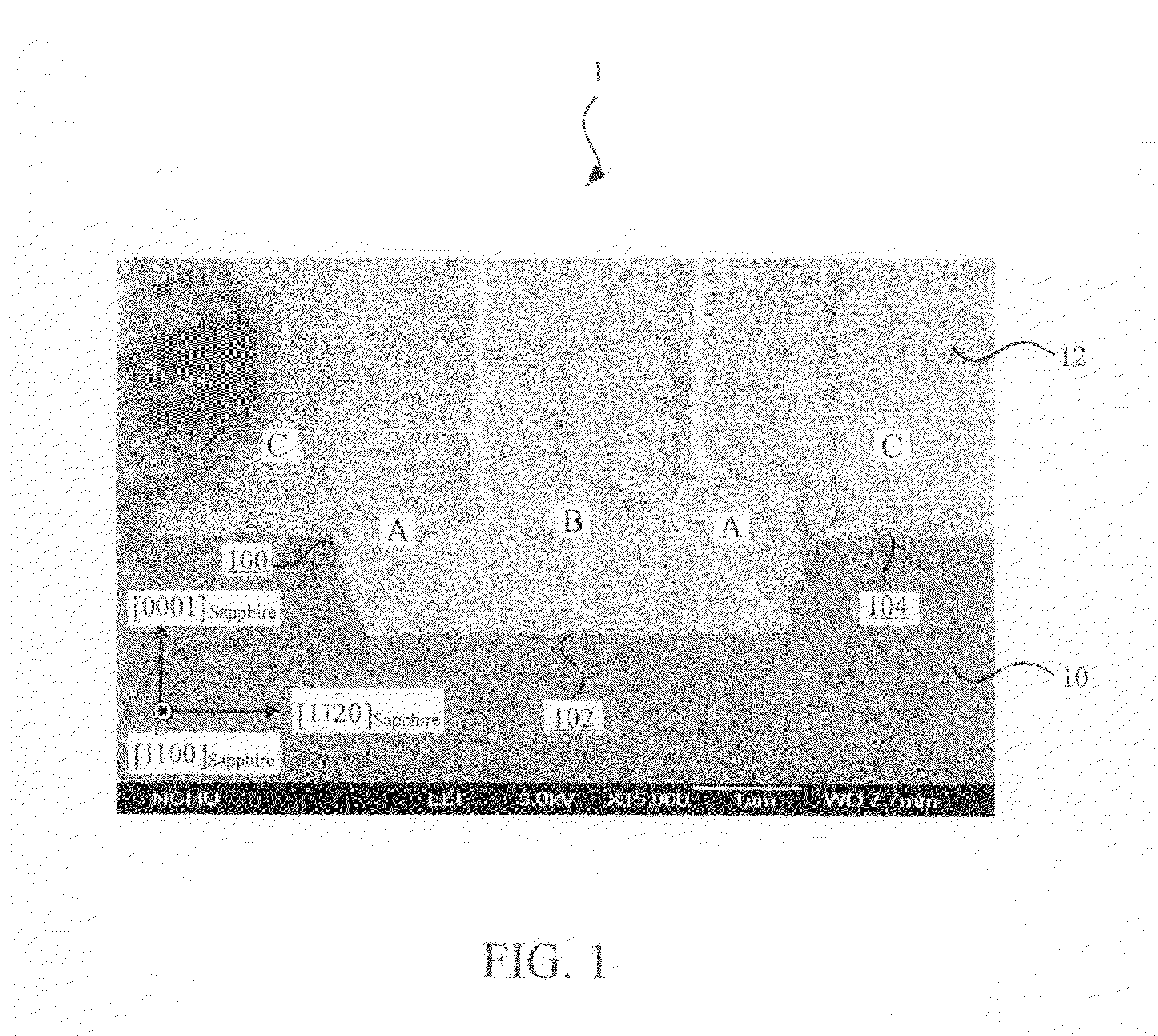
[0030]Please refer to FIG. 1. FIG. 1 is an SEM cross-sectional view of a semiconductor structure combination 1 according to an embodiment of the invention for the epitaxy of a semiconductor optoelectronic device.

[0031]The semiconductor structure combination 1 includes a substrate 10, at least one first epitaxial crystal A of a semiconductor material 12, a second epitaxial crystal B of the semiconductor material 12, and at least one third epitaxial crystal C of the semiconductor material 12. The substrate 10 has an upper surface and a recess formed on the upper surface.

[0032]In practical applications, the substrate 10 can be Si, SiO2, GaN, AlN, sapphire, spinner, SiC, GaAs, Al2O3, LiGaO2, LiAlO2, or MgAl2O4.

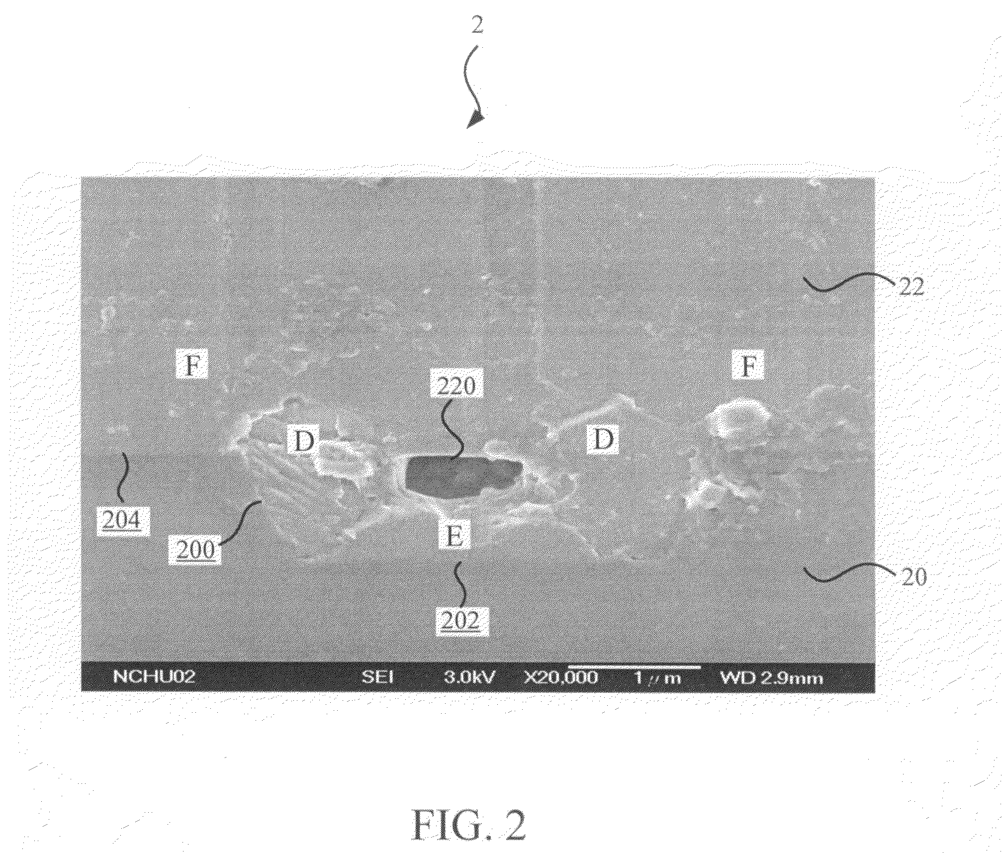
[0033]Sidewalls 100 of the recess provide at least one first site for the growth of a semiconductor material 12 toward a first preferred orientation. A bottom 102 of the recess provides a second site for the growth of the semiconductor material 12 toward the first preferred orient...


PUM


Abstract

The invention discloses a semiconductor structure combination for the epitaxy of a semiconductor optoelectronic device and manufacture thereof. The semiconductor structure combination according to the invention includes a substrate and a semiconductor material. The substrate has an upper surface and a recess formed on the upper surface. The sidewalls of the recess provide at least one first site for the growth of at least one first epitaxial crystal of the semiconductor material toward a first preferred orientation. A bottom of the recess provides a second site for the growth of a second epitaxial crystal of the semiconductor material toward the first preferred orientation. Flat regions adjacent to the recess provide at least one third site for the growth of at least one third epitaxial crystal of the semiconductor material toward the first preferred orientation.

Description

BACKGROUND OF THE INVENTION[0001]1. Field of the Invention[0002]The present invention relates to a semiconductor structure combination and, more particularly, to a semiconductor structure combination for a semiconductor optoelectronic device.[0003]2. Description of the Prior Art[0004]The current semiconductor light-emitting devices, such as light-emitting diodes, have been used for a wide variety of applications, e.g. illumination, remote control. To ensure high functional reliability as great as possible and a low power requirement of the semiconductor light-emitting devices, the external quantum efficiency is required for the devices.[0005]In theory, the external quantum efficiency of a semiconductor light-emitting device is determined by the internal quantum efficiency thereof. The internal quantum efficiency is determined by the material property and quality. If a density of inner defects of the semiconductor light-emitting device becomes higher, it will lower the internal quant...

Claims


Application Information

Patent Timeline
Patent Type & Authority Applications(United States)
IPC IPC(8): H01L33/00
CPCH01L21/02378H01L21/02381H01L21/02389H01L21/02395H01L33/007H01L21/02433H01L21/02538H01L21/02609H01L21/0262H01L21/0242
Inventor CHENG, CHIH-CHINGTSAI, TZONG-LIANG
Owner EPISTAR CORP
Why Eureka
Try Eureka