Infrared photosensor

a photosensor and thermal imaging technology, applied in the direction of diodes, radiation control devices, semiconductor devices, etc., can solve the problems of thermal diode noise, thermal noise of the thermal diode, current noise, etc., to improve the absorption of infrared radiation, reduce the density of defects at the interface between the absorption layer and an adjacent layer, and facilitate the manufacturing process.

Active Publication Date: 2014-04-03
ROBERT BOSCH GMBH
View PDF10 Cites 2 Cited by
  • Summary
  • Abstract
  • Description
  • Claims
  • Application Information

AI Technical Summary

Benefits of technology

[0016]In another specific embodiment, the base may be doped differently from the first or second structure. This allows the use of a doped semiconductor substrate or a layer of a doped semiconductor substrate on the undoped semiconductor substrate. In addition, the base may be manufacturable separately from the first or second doped structure, which means a manufacturing process is able to be made easier.
[0017]An absorption layer may be provided to cover the structures and the area situated between them on the surface of the semiconductor substrate, the absorption layer having a thickness modulated subject to the process, especially a uniform thickness. For example, the absorption layer may include silicon dioxide in order to improve absorption of the infrared radiation to be detected. By forming the absorption layer in a uniform thickness, the density of defects at the interface between the absorption layer and an adjacent layer may be reduced. In addition, different current paths are able to have more uniform lengths, that is, variance in the lengths of all current paths may be reduced. The 1 / f noise is thereby able to be reduced overall.
[0018]In one specific embodiment, one surface of the absorption layer may be even. Furthermore, the thickness of the absorption layer may not exceed 50 nm. In one specific embodiment, the absorption layer may reach a layer thickness of no more than 20 nm. Due to a reduced layer thickness, a reduced impurity concentration may be obtained, which means the 1 / f noise may therefore be reduced overall.

Problems solved by technology

The noise of the thermal diode usually includes thermal noise, shot noise and 1 / f noise.
The 1 / f noise of the thermal diode is produced in particular by structure defects within the semiconductor material or at an interface of the semiconductor material of the thermal diode.
The entrance of a charge carrier into and its exit from such a defect alters the current flowing through the thermal diode and thus produces a current noise.

Method used


Image

  • Infrared photosensor
  • Infrared photosensor
  • Infrared photosensor

Examples


Embodiment Construction

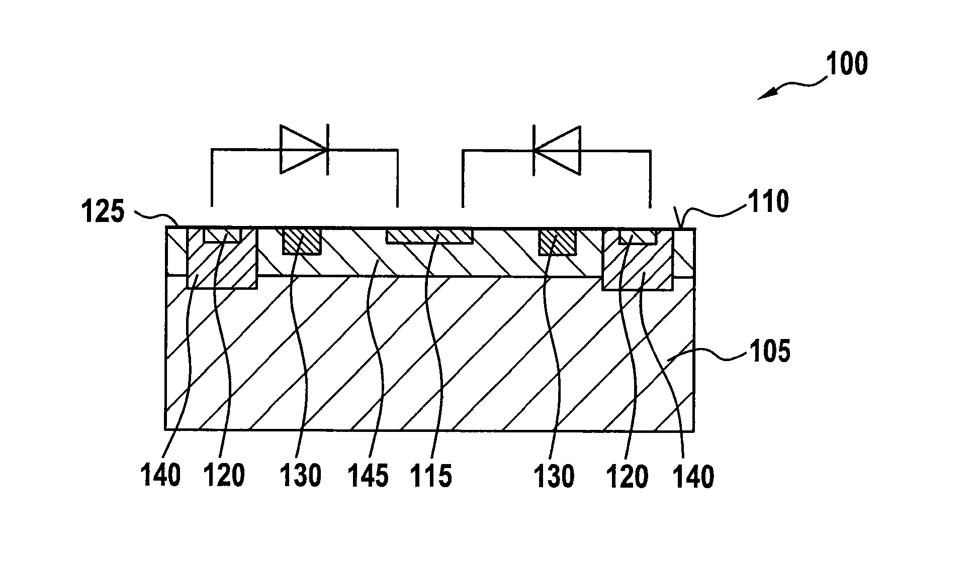
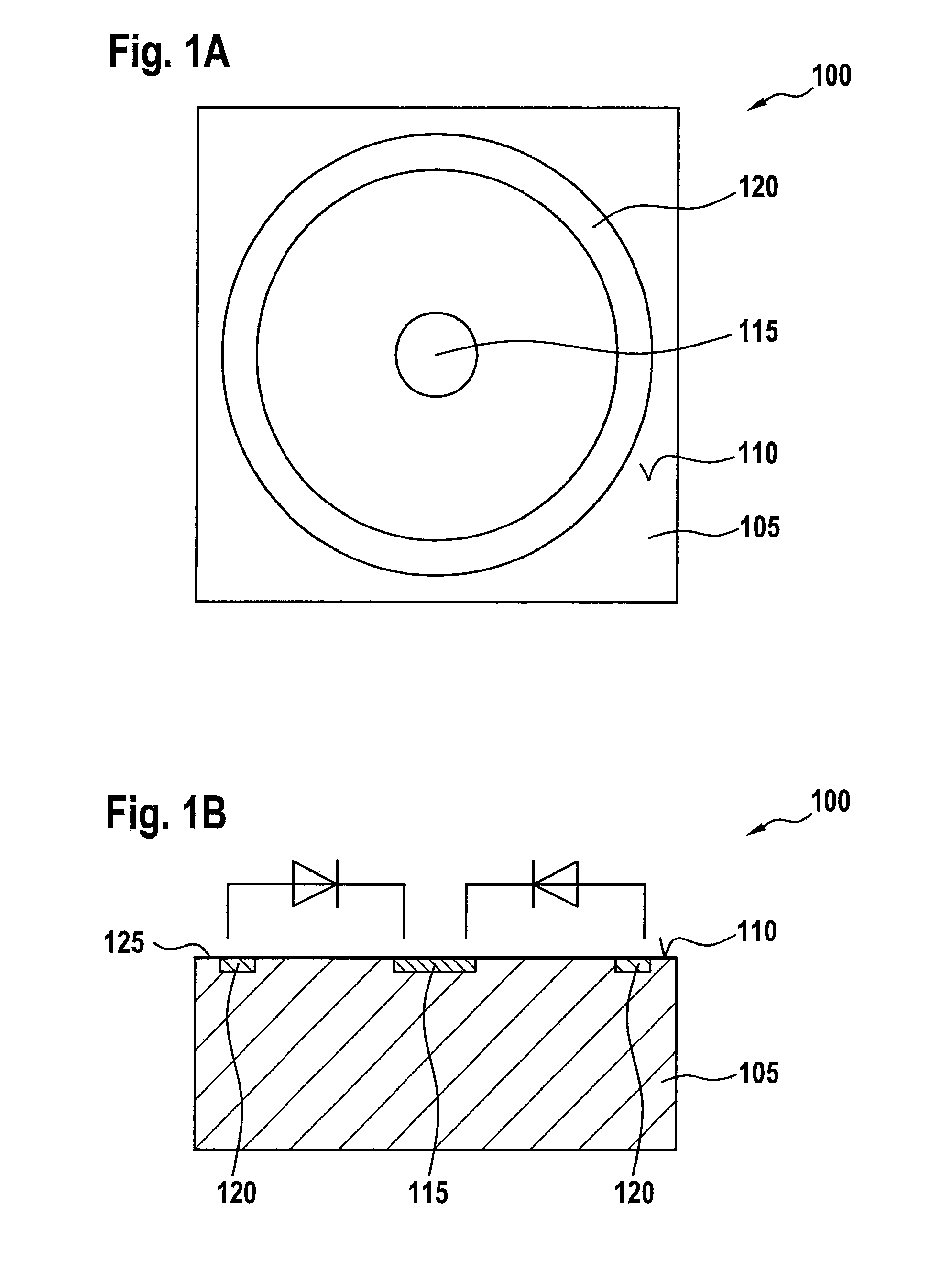
[0028]FIG. 1A shows a top view and FIG. 1B shows a lateral view of thermal diode 100. In the specific embodiment shown, a concentric, especially a circular concentric formation is selected. In other specific embodiments, other concentric or linear formations may also be used.

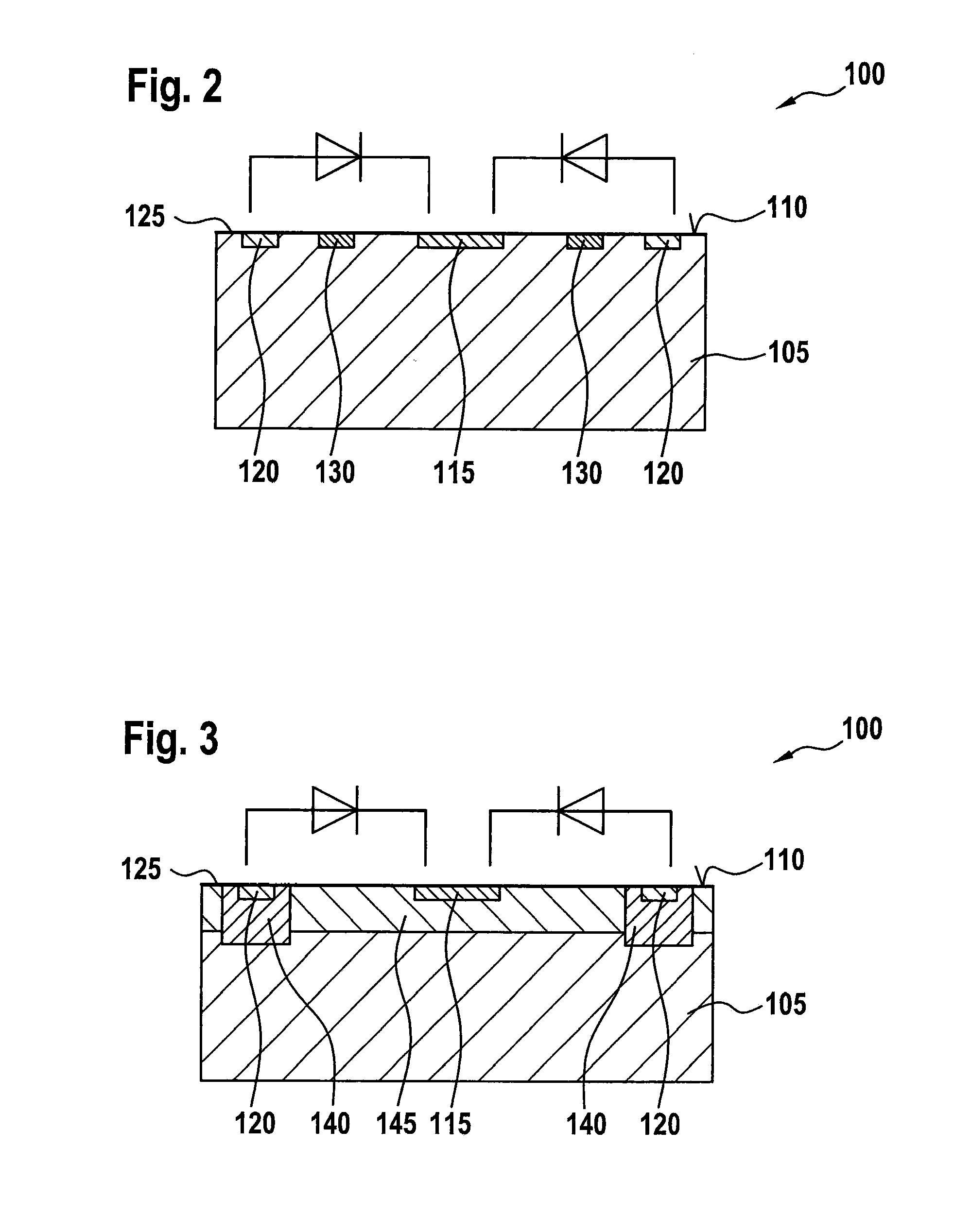
[0029]A substrate 105 of semiconductor material, e.g., silicon (Si), has a surface 110 on which a first doped structure 115 and a second doped structure 120 are disposed. In this context, structures 115 and 120 on surface 110 may be embedded into substrate 105, as illustrated in FIG. 1B. Structures 115 and 120 as well as the area of surface 110 of substrate 105 may be situated between them are covered uppermost with an absorption layer 125. For example, absorption layer 125 may be formed of silicon dioxide (SiO2).

[0030]Structures 115 and 120 are doped with different polarity; for instance, first structure 115 may be N-doped, while second structure 120 is P-doped. A reversed polarity is likewise possible. A diode...


PUM


Abstract

A thermal diode for a photosensor of a thermal imaging camera includes a semiconductor substrate having a surface and two doped structures set apart from each other on the surface. Furthermore, a device is provided for influencing a current between the first and the second structure, in order to reduce a current density in an area near to the surface and to increase it in an area far from the surface. In addition, a topology having an even absorption layer is proposed. The measures proposed have the aim of realizing a low-noise diode for thermal applications.

Description

RELATED APPLICATION INFORMATION[0001]The present application claims priority to and the benefit of German patent application no. 10 2012 216 814.1, which was filed in Germany on Sep. 19, 2012, the disclosure of which is incorporated herein by reference.FIELD OF THE INVENTION[0002]The present invention relates to a photosensor for a thermal imaging camera. In particular, the invention relates to a thermally sensitive diode for the photosensor.BACKGROUND INFORMATION[0003]A thermal imaging camera for spatially-resolved temperature measurement uses a thermally sensitive sensor array, in which a characteristic thermal radiation of an object is imaged onto an array of thermally sensitive sensor elements by a lens transmitting infrared radiation. For example, long-wave infrared radiation (LWIR) includes wavelengths in the range of approximately 8 to 14 μm. Due to the infrared radiation, the sensor elements warm up by amounts on the order of a few mK. An uncooled sensor array for characteri...

Claims


Application Information

Patent Timeline
Patent Type & Authority Applications(United States)
IPC IPC(8): H01L27/146H01L31/102
CPCH01L31/102H01L27/14649H01L27/14601H01L27/14603H01L27/14643H01L31/00H01L31/0352H01L31/103
Inventor SENZ, VOLKMARKRUEGER, MICHAEL
Owner ROBERT BOSCH GMBH
Why Eureka
Try Eureka