Process for producing SOI substrate and process for regeneration of layer transferred wafer in the production

a technology of silicon on insulator and substrate, which is applied in the direction of crystal growth process, polycrystalline material growth, after-treatment details, etc., can solve the problems of increased leak current and the like of a manufactured device, wire disconnection, and failure to meet the requirements of the manufacturing process, so as to achieve the effect of reducing the substantial vacancy concentration, and reducing the generation probability of oxygen precipitates

Inactive Publication Date: 2010-09-07
SUMCO CORP
View PDF18 Cites 2 Cited by
  • Summary
  • Abstract
  • Description
  • Claims
  • Application Information

AI Technical Summary

Benefits of technology

[0010]Accordingly, the object of the present invention is to provide a process for producing an SOI substrate for preventing oxygen precipitates from occurring in an SOI substrate obtained by reusing a layer transferred wafer. Additionally, the object of the present invention is to provide a process for the regeneration of a layer transferred wafer in the production.
[0013]In the process for producing an SOI substrate according to the first embodiment of the present invention, the ingot for preparing the first silicon substrate 14 is grown in an inorganic atmosphere including hydrogen, and the perfect area [P] thereof increases. It is possible to relatively easily obtain the first silicon substrate 14 free of an agglomerate of vacancy type point defects and an agglomerate of interstitial silicon type point defects, and so, it is possible to decrease the unit price of the obtained SOI substrate 11.
[0014]Further, a wafer free of an agglomerate of vacancy type point defects and an agglomerate of interstitial silicon type point defects is used as the first silicon substrate 14, and accordingly, solid solution oxygen that causes crystal defects of the SOI layer 13 hardly becomes oxygen precipitates in the heat treatment. Furthermore, in a hydrogen doped ingot, the COP size becomes smaller even in an area where COPs exist. COPs easily cease to exist in the heat treatment in a reduction atmosphere of the producing process of the SOI substrate. Moreover, by hydrogen doping, vacancy type point defects necessary for the generation and growth of oxygen precipitates are united with hydrogen and the substantial vacancy concentration decreases, and so, in comparison with a normal crystal, the generation probability of oxygen precipitates becomes further smaller. Accordingly, it is possible to prevent oxygen precipitates and COPs from occurring in the SOI layer 13 in the SOI substrate 11 obtained by this producing process and the SOI layer 13 in the SOI substrate 11 using a layer transferred wafer by-produced by this process as the first silicon substrate 14. The defect density in these SOI layers 13 decreases from that in the conventional one, and the crystal quality of the SOI layers 13 in these SOI substrates 11 can be improved further.
[0018]In the process for the regeneration of a layer transferred wafer in the production of an SOI substrate according to this embodiment, the layer transferred wafer 17 is obtained by separating the first silicon substrate 14 formed by slicing an ingot free of an agglomerate of vacancy type point defects and an agglomerate of interstitial silicon type point defects. Accordingly, even in the obtained layer transferred wafer 17, in comparison with a normal crystal, the generation probability of oxygen precipitates becomes smaller. Further, by a crystal pulled up in an atmosphere including hydrogen, vacancy type point defects necessary for the generation and growth of oxygen precipitates are united with hydrogen and the substantial vacancy concentration decreases, and so, in comparison with a normal crystal, the generation probability of oxygen precipitates becomes further smaller. Accordingly, even when an SOI substrate is produced once again by using this layer transferred wafer 17 as the first silicon substrate 14, it is prevented crystal defects from occurring in the SOI layer in the obtained SOI substrate 11, and so, it is possible to increase the number of regeneration times than that in the case of a normal crystal without deteriorating the crystal quality of the obtained SOI layer 13.
[0019]In the process for producing an SOI substrate according to the present invention, because a first silicon substrate is formed by slicing an ingot free of an agglomerate of vacancy type point defects and an agglomerate of interstitial silicon type point defects grown by a CZ method in an inorganic atmosphere including hydrogen, the perfect area [P] of the ingot increases, and so, it is possible to relatively easily obtain a first silicon substrate free of the agglomerate of vacancy type point defects and the agglomerate of interstitial silicon type point defects. As a result, it is possible to decrease the unit price of the obtained SOI substrate 11. And, because a wafer free of an agglomerate of vacancy type point defects and an agglomerate of interstitial silicon type point defects is used as a first silicon substrate, and hydrogen is doped, vacancy type point defects necessary for the generation and growth of oxygen precipitates are united with hydrogen and the substantial vacancy concentration decreases. Thus, in comparison with a normal crystal, the generation probability of oxygen precipitates becomes further smaller. Accordingly, solid solution oxygen that causes crystal defects of the SOI layer hardly becomes oxygen precipitates in the heat treatment, and the COP size becomes smaller even in an area where COPs exist. Accordingly, it is possible to prevent COPs from occurring in the SOI layer in the SOI substrate 11 obtained by this producing process and the SOI layer in the SOI substrate using a layer transferred wafer by-produced by this producing process as a first silicon substrate, and to further improve the crystal quality of the SOI layers in these SOI substrates.
[0020]Further, in the process for regeneration of a layer transferred wafer in the production of an SOI substrate by the use of a layer transferred wafer separated from an SOI layer by separating at the ion implantation area in a process for producing an SOI substrate, even in an obtained layer transferred wafer, in comparison with a normal crystal, the generation probability of oxygen precipitates becomes smaller. Accordingly, even when an SOI substrate is produced once again by using this layer transferred wafer as a first silicon substrate, it is prevented crystal defects from occurring in the SOI layer in the obtained SOI substrate, and so, it is possible to increase the number of regeneration times than that in the case of a normal crystal without deteriorating the crystal quality of the obtained SOI layer.

Problems solved by technology

Specifically, micro defects to become nuclei of this OSF are introduced into a crystal at the growth of the crystal, and this OSF becomes obvious in a thermal oxidation process or the like in producing a semiconductor device and causes failures including increased leak current and the like of a manufactured device.
Further, if there is a COP on a wafer surface, a dump occurs in a device wiring process, leading to a wire disconnection.
And in an element separation portion too, the COP causes a leak and the like, decreasing the yield of products.
This L / D also causes the deterioration of electric characteristics such as, for example leak characteristics, isolation characteristics and the like.
However, when a wafer free of crystal defects sliced from an ingot not hydrogen doped is used as a first silicon substrate, there is a fear that oxygen existing in solid solution form in the first silicon substrate may become oxygen precipitates in plural times of heat treatment in the production process.
Therefore, even if an SOI substrate is produced by use of a wafer free of crystal defects sliced from an ingot not hydrogen doped is used as a first silicon substrate, oxygen precipitates may occur in a layer transferred wafer by-produced at the production thereof, and so, oxygen precipitates may exist in an SOI substrate obtained by reusing the layer transferred wafer as a first silicon substrate, which has been a problem not solved yet in the prior art.

Method used


Image

  • Process for producing SOI substrate and process for regeneration of layer transferred wafer in the production
  • Process for producing SOI substrate and process for regeneration of layer transferred wafer in the production
  • Process for producing SOI substrate and process for regeneration of layer transferred wafer in the production

Examples


example 1

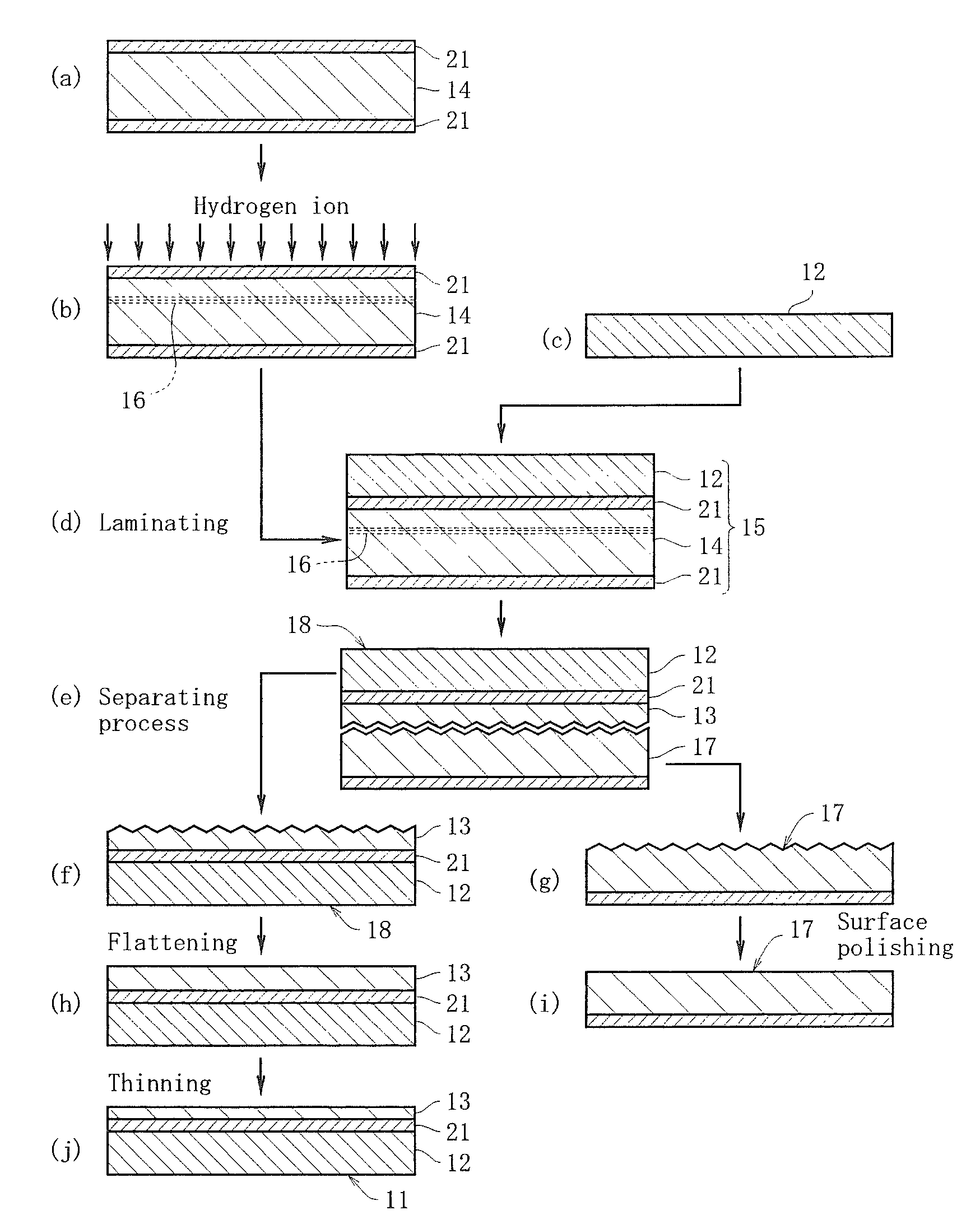
[0049]A boron (B) doped p-type silicon ingot of a diameter 8 inch was pulled up by the CZ method in an inorganic atmosphere including hydrogen by use of a silicon single crystal puller. Into the inside of the puller, argon gas was flown at the flow amount 40 litters / minute, from the moment of heating the raw material to the moment of cooling the raw material. After poly silicon of the raw material started melting, until the ingot was pulled up completely, hydrogen gas whose volume ratio to that of argon gas was 6% was mixed from the inlet port of argon gas and guided into the puller. With regard to the ingot pulled up, the resistance ratio is approximately 10 Ωcm, and the oxygen concentration is 5×10¹⁷ atoms / cm3. Two ingots were grown under the same conditions, while the V / G at the pulling moment was continuously decreased from 0.24 mm2 / minute·° C. to 0.18 mm2 / minute·° C. With regard to one ingot among the two ingots, the ingot center was cut in the pulling direction as shown in FIG...

example 2

[0053]With regard to the layer transferred wafer (FIG. 1(g)) obtained by performing the heat treatment onto the laminated body 15 and cutting the same at the ion implantation area 16 in Example 1, the separated surface from the SOI layer 13 was polished (FIG. 1(i)). The layer transferred wafer 17 where this separated surface was polished was used once again as a first silicon substrate 14, and by the same conditions and procedures as those in Example 1, an SOI substrate 11 was obtained again. This SOI substrate 11 obtained once again was made as Example 2.

example 3

[0054]With regard to the layer transferred wafer (FIG. 1(g)) obtained by performing the heat treatment onto the laminated body 15 and cutting the same at the ion implantation area 16 in Example 2, the separated surface from the SOI layer 13 was polished (FIG. 1(i)). The layer transferred wafer 17 where this separated surface was polished was used once again as a first silicon substrate 14, and by the same conditions and procedures as those in Example 1, a third SOI substrate 11 was obtained. This SOI substrate 11 obtained thirdly was made as Example 3.


PUM

PropertyMeasurementUnit
volume %aaaaaaaaaa
volume %aaaaaaaaaa
temperatureaaaaaaaaaa

Abstract

A process for producing an SOI substrate includes the steps of forming an oxide film on at least the front surface of a first silicon substrate, implanting hydrogen ion from the surface of the first silicon substrate and thereby forming an ion implantation area in the inside of the first silicon substrate, laminating a second silicon substrate onto the first silicon substrate via the oxide film and thereby forming a laminated body of the first silicon substrate and the second silicon substrate bonded with each other, and heating the laminated body at a predetermined temperature and thereby separating the first silicon substrate at the ion implantation area and thereby obtaining an SOI substrate wherein a thin film SOI layer is formed on the second silicon substrate via the oxide film. The first silicon substrate is formed by slicing an ingot free of an agglomerate of vacancy type point defects and an agglomerate of interstitial silicon type point defects grown by a CZ method in an inorganic atmosphere including hydrogen. The layer transferred wafer separated from the SOI layer is used again as the first silicon substrate.

Description

CROSS-REFERENCES TO RELATED APPLICATIONS[0001]This application claims priority under 35 U.S.C. §119(d) to Japanese Application No. 2005-110828 filed Apr. 7, 2005, the entire disclosure of which is hereby incorporated by reference.BACKGROUND OF THE INVENTION[0002]1. Field of the Invention[0003]The present invention relates to a process for producing an SOI (Silicon On Insulator) substrate in which an SOI layer is manufactured on an oxide film by use of hydrogen ion implantation technology. Additionally, the present invention relates to a process for the regeneration of a layer transferred wafer in the process for producing an SOI.[0004]2. Description of the Related Art[0005]Conventionally, a process for producing an SOI substrate has been known in which after an oxide film is formed on the surface of a first silicon substrate, hydrogen ions of a high concentration are implanted into the inside thereof, and an annealing process is performed at a high temperature. Additionally, a hydro...

Claims


Application Information

Patent Timeline
Patent Type & Authority Patents(United States)
IPC IPC(8): H01L21/22
CPCC30B29/06C30B33/00H01L21/02032H01L21/76254H01L21/20H01L27/12
Inventor ENDO, AKIHIKOONO, TOSHIAKISUGIMURA, WATARU
Owner SUMCO CORP
Why Eureka
Try Eureka