Laminate type electronic component

Inactive Publication Date: 2005-04-21
TDK CORPARATION
View PDF4 Cites 33 Cited by
  • Summary
  • Abstract
  • Description
  • Claims
  • Application Information

AI Technical Summary

Benefits of technology

[0051] When the resin electrode layer and the dielectric part are connected to each other by way of the metal electrode layer, the electric contact state between the resin electrode layer and the internal electrode in the dielectric part can be made better than that in the case where the resin electrode layer is directly formed on the surface of the dielectric part, whereby the electric contact resistance between the resin electrode layer and the dielectric part occurring when the resin electrode layer is directly formed on the surface of the dielectric powder can sufficiently be lowered in an easy and reliable manner. Also, by way of the metal electrode layer, the resin electrode layer can physically be secured to the dielectric part more firmly.
[0052] When the metal electrode layer is provided, it will be preferred that the metal electrode layer is formed by sintering a paste mainly composed of any of metals of Cu, Ag, Pd, Ni, and Ag—Pd alloy, from the viewpoint of sufficiently lowering the above-mentioned electric resistance and from the viewpoint of manufacturing efficiency.
[0053] Preferably, in the present invention, a Ni plating layer formed from Ni by plating is further disposed on an out

Problems solved by technology

However, when employed in a power supply bypass circuit, all of the conventional electronic components such as those mentioned above are quite hard to sufficiently prevent the oscillation phenomenon from occurring and achieve a sufficient smoothing action, and fail to attain a sufficient reliability.
Also, the above-mentioned electronic components include those having a configuration which is poor in mass productivity.
HEI 8-45784, manufacturing conditions for accurately regulating its resistance value within a desirable range and a manufacturing step for satisfying the conditions become quite complicated, so that a desirable resistance value is hard to attain accurately, circuits a

Method used


Image

  • Laminate type electronic component
  • Laminate type electronic component
  • Laminate type electronic component

Examples


example 1

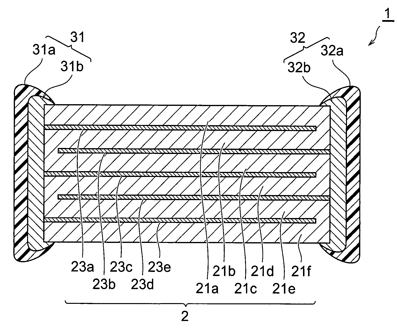
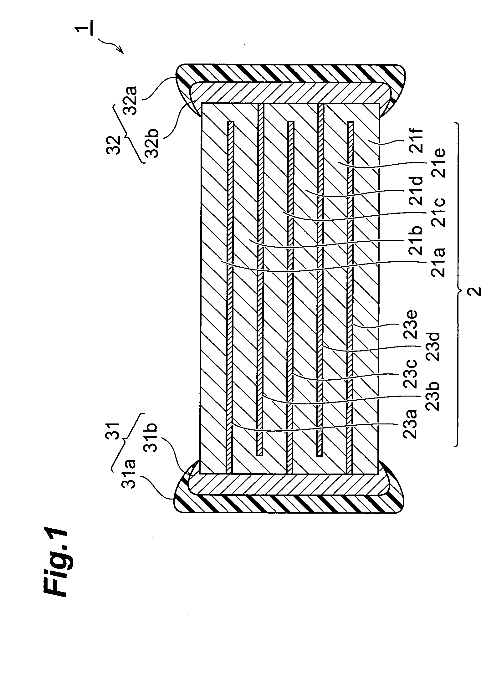
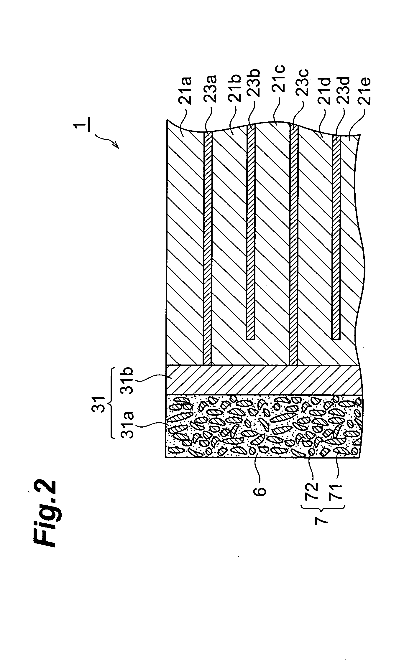
[0079] In the following procedure, the laminated ceramic capacitor shown in FIGS. 1 and 2 was made.

[0080] First, using 110 dielectric layers (in each of which a dielectric to become a constituent material was mainly composed of BaTiO3 with a thickness of 2 to 10 μm) having a rectangular parallelepiped shape, and internal electrodes, each formed like a rectangular plate (with a thickness of 1 to 2 μm) made of Ni, disposed one by one between two layers adjacent each other among the dielectric layers, a laminate (green sheet) made of 110 dielectric layers having a configuration in which the internal electrodes alternated with the dielectric layers was made by a known manufacturing technique.

[0081] More specifically, a paste containing a dielectric material was prepared, and then each dielectric layer was formed from this paste by doctor blading. Each internal electrode comprising Ni was formed by preparing a Ni paste mainly composed of Ni and then printing this paste on each dielectr...

examples 2 and 3

[0088] Laminated ceramic capacitors were made in the same procedure under the same condition as with Example 1 except that respective conductive particle contents in each of the resin electrode layers in the first and second external electrodes were adjusted to their corresponding values shown in Table 1, and that respective particles having their corresponding aspect ratios and average longitudinal lengths shown in Table 1 were used as the acicular particles (particles made of Ag).

examples 4 to 15

[0089] Laminated ceramic capacitors were made in the same procedure under the same condition as with Example 1 except that respective conductive particle contents in each of the resin electrode layers in the first and second external electrodes were adjusted to their corresponding values shown in Table 1, that respective particles having their corresponding aspect ratios and average longitudinal lengths shown in Table 1 were used as the acicular particles (particles made of Ag), and that respective particles having their corresponding average particle sizes shown in Table 1 were used as spherical particles (particles made of Ag).


PUM


Abstract

A laminate type electronic component 1 comprises, at least, a dielectric part 2 containing a dielectric as a constituent material, and a pair of a first external electrode 31 and a second external electrode 32, each disposed in close contact with the dielectric part 2, opposing each other by way of the dielectric part 2. The dielectric part 2 comprises laminated dielectric layers 21a to 21f; and at least two internal electrodes 23a to 23e disposed one by one between layers adjacent each other in the dielectric layers 21a to 21f, while each being electrically connected to one of the first external electrode 31 and second external electrode 32. At least one of the internal electrodes 23a to 23e is electrically connected to the first external electrode 31, and at least one of the internal electrodes 23a to 23e is electrically connected to the second external electrode 32.
The first external electrode 31 and second external electrode 32 comprise resin electrode layers 31a and 32a, each made of a conductive resin mainly composed of a thermosetting resin and a conductive particle; a metal electrode layer 31b disposed between the resin electrode layer 31a and the dielectric part 2; and a metal electrode layer 32b disposed between the resin electrode layer 32a and the dielectric part 2. The conductive particle content in the conductive resin is 70 to 75 mass %, whereas the conductive particle contains, as a main ingredient, acicular particles 71 having an average longitudinal length of 30 to 70 μm and an aspect ratio of 1.5 to 3.3.

Description

TECHNICAL FIELD [0001] The present invention relates to a laminate type electronic component and, more specifically, to a laminate type electronic component such as a laminated ceramic capacitor. BACKGROUND ART [0002] Switching power supplies and DC / DC converters have currently been employed in many of power supplies of electronic devices. Known as a capacitor used in these power supplies is a power supply bypass capacitor. [0003] For the power supply bypass capacitor, an aluminum electrolytic capacitor or tantalum electrolytic capacitor having a large capacity or a laminated ceramic capacitor having a low capacity has been used according to circuit parameters such as its power capacity and switching frequency and a smoothing coil employed. [0004] Though the electrolytic capacitors mentioned above have excellent advantages in that they can easily attain a large capacity as a power supply bypass (smoothing) capacitor, they are problematic in that they are large in size; they are poor...

Claims


Application Information

Patent Timeline
IPC IPC(8): H01G4/06H01G4/232H01G4/30H02B1/00
CPCH01G4/2325
Inventor YOSHLL, AKITOSHIYOKOYAMA, HIDEKIKAMIYA, TAKASHITAKEDA, ATSUSHIOKABE, MASAYUKI
Owner TDK CORPARATION
Why Eureka
Try Eureka